Semiconductor device with capacitor
A technology of capacitors and semiconductors, which is applied to semiconductor devices, electric solid devices, semiconductor/solid device components, etc., can solve problems such as mutual interference and waste of wafer area, and achieve the effect of avoiding mutual interference
- Summary
- Abstract
- Description
- Claims
- Application Information
AI Technical Summary
Benefits of technology
Problems solved by technology
Method used
Image

Examples
Embodiment Construction
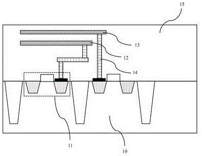
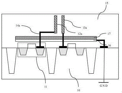
[0022] see figure 2 , the present invention provides a semiconductor device with a capacitor, which has a plurality of functional devices 11 on the upper surface of a semiconductor substrate 10, and the functional devices 11 may be transistors; a MIM capacitor formed on the functional device 11; wherein, the The MIM capacitor is perpendicular to the upper surface and covered by an insulating layer 15, the insulating layer is a single silicon oxide material, and a part of the insulating layer 15 is used as a dielectric layer of the capacitor. The MIM capacitor includes a first metal plate 12a and a second metal plate 13a perpendicular to the upper surface and an insulating layer between the first and second metal plates 12a, 13a.
[0023] There is a shielding layer 16 between the MIM capacitor and the functional device 11 , the shielding layer 16 is a grounded metal layer made of conductive hard metal such as copper, titanium, aluminum, nickel and the like.
[0024] A stress buf
PUM
 Abstract
Description
Claims
Application Information
 - R&D Engineer
- R&D Manager
- IP Professional
- Industry Leading Data Capabilities
- Powerful AI technology
- Patent DNA Extraction
Browse by: Latest US Patents, China's latest patents, Technical Efficacy Thesaurus, Application Domain, Technology Topic.
© 2024 PatSnap. All rights reserved.Legal|Privacy policy|Modern Slavery Act Transparency Statement|Sitemap