Brazing filler metal for brazing 3D printing stainless steel and silicon nitride ceramic and brazing method
A technology of silicon nitride ceramics and 3D printing, which is applied in the direction of welding/cutting media/materials, welding media, welding equipment, etc., can solve the problems of large stress concentration in the welding layer and large difference in linear expansion coefficient, etc. Good corrosion resistance, good wettability and spreading effect
- Summary
- Abstract
- Description
- Claims
- Application Information
AI Technical Summary
Problems solved by technology
Method used
Image

Examples
Example Embodiment
[0017] Example 1
[0018] Choose 3D printed stainless steel and silicon nitride ceramics for vacuum brazing of butt joints. The dimensions of the 3D printed stainless steel and silicon nitride ceramics are both 20mm×20mm×5mm, and the brazing surface is 20mm×5mm.
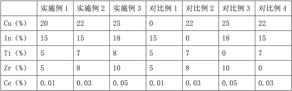
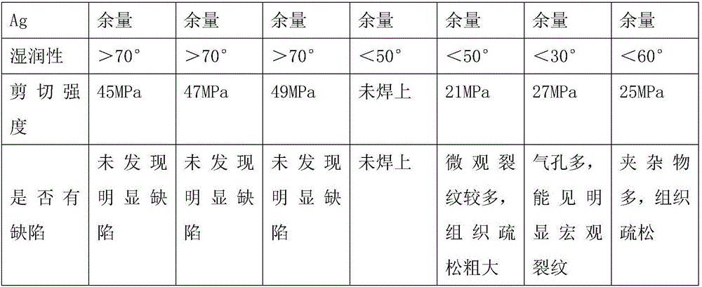
[0019] The composition and mass percentage ratio of the solder are: Cu20.0%, In15.0%, Ti5.0%, Zr5.0%, Ce0.01%, and the balance is Ag. The thickness of the solder is 60μm and the thickness of the copper foil is 60μm. The brazing process steps are:
[0020] (1) Preparation stage: clean the end faces of the 3D printed stainless steel and silicon nitride ceramic samples to be welded to remove surface impurities, oil stains and oxide films. Use W40~W7 metallographic sandpaper to grind and smooth the 3D printed stainless steel. W7 metallographic sandpaper grinds both sides of the solder foil and copper foil smoothly. After grinding, put the sample to be soldered, solder and copper foil together in acetone, clean it with ultrasonic
Example Embodiment
[0024] Example 2
[0025] 3D printing stainless steel and silicon nitride ceramics for vacuum brazing of butt joints. The dimensions of the 3D printed stainless steel and silicon nitride ceramics are both 20mm×20mm×5mm, and the brazing surface is 20mm×5mm.
[0026] The composition and mass percentage ratio of the solder are: Cu22.0%, In16.0%, Ti7.0%, Zr8.0%, Ce0.03%, and the balance is Ag. The thickness of the provided solder is 80μm, and the thickness of the copper foil is 70μm. The brazing process steps are:
[0027] (1) Preparation stage: clean the end faces of the 3D printed stainless steel and silicon nitride ceramic samples to be welded to remove surface impurities, oil stains and oxide films. Use W40~W7 metallographic sandpaper to grind and smooth the 3D printed stainless steel. W7 metallographic sandpaper grinds both sides of the solder foil and copper foil smoothly. After grinding, put the sample to be soldered, solder and copper foil together in acetone, clean it with ultras
Example Embodiment
[0031] Example 3
[0032] Choose 3D printed stainless steel and silicon nitride ceramics for vacuum brazing of butt joints. The dimensions of the 3D printed stainless steel and silicon nitride ceramics are both 20mm×20mm×5mm, and the brazing surface is 20mm×5mm.
[0033] The composition and mass percentage ratio of the solder is: Cu25.0%, In18.0%, Ti8.0%, Zr10.0%, Ce0.05%, and the balance is Ag. The thickness of the provided solder is 150μm, and the thickness of the copper foil is 80μm.
[0034] The brazing process steps are:
[0035] (1) Preparation stage: clean the end faces of the 3D printed stainless steel and silicon nitride ceramic samples to be welded to remove surface impurities, oil stains and oxide films. Use W40~W7 metallographic sandpaper to grind and smooth the 3D printed stainless steel. W7 metallographic sandpaper grinds both sides of the solder foil and copper foil smoothly. After grinding, put the sample to be soldered, solder and copper foil together in acetone, clean
PUM
| Property | Measurement | Unit |
|---|---|---|
| Thickness | aaaaa | aaaaa |
| Thickness | aaaaa | aaaaa |
| Room temperature shear strength | aaaaa | aaaaa |
Abstract
Description
Claims
Application Information
 - R&D Engineer
- R&D Manager
- IP Professional
- Industry Leading Data Capabilities
- Powerful AI technology
- Patent DNA Extraction
Browse by: Latest US Patents, China's latest patents, Technical Efficacy Thesaurus, Application Domain, Technology Topic.
© 2024 PatSnap. All rights reserved.Legal|Privacy policy|Modern Slavery Act Transparency Statement|Sitemap