Display panel and display device

A display panel and display area technology, applied in static indicators, instruments, etc., can solve the problem of uneven display, reduce the load gap, improve the uneven data writing, and alleviate the uneven display effect.

Inactive Publication Date: 2017-12-15
WUHAN TIANMA MICRO ELECTRONICS CO LTD
View PDF4 Cites 103 Cited by
  • Summary
  • Abstract
  • Description
  • Claims
  • Application Information

AI Technical Summary

Problems solved by technology

[0003] Embodiments of the present invention provide a display panel and a display device, which

Method used


Image

  • Display panel and display device
  • Display panel and display device
  • Display panel and display device

Examples


Embodiment Construction

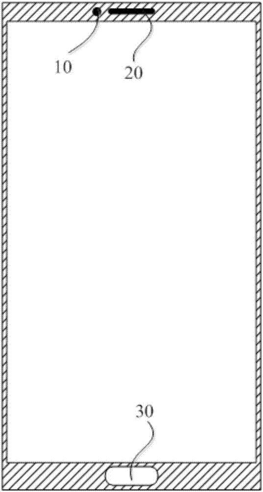
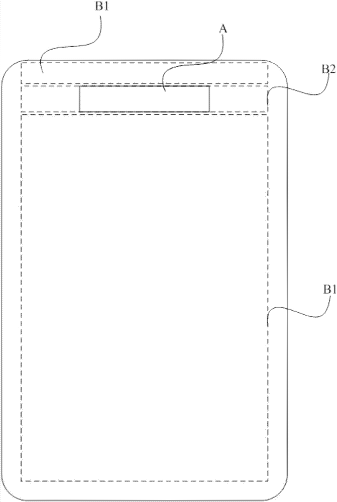
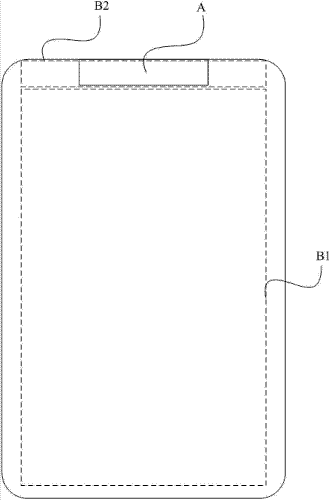
[0045] In order to achieve full screen display, such as Figure 2a and Figure 2b As shown, devices such as cameras and earpieces are generally arranged in the special-shaped area A of the display panel, so that the number of pixels in a row of pixels in the first display area B1 of the display panel is greater than the number of pixels in a row of pixels in the second display area B2. Among them, the second display area B2 is an area adjacent to the left and right of the heterogeneous area A, resulting in different loads on the scanning signal lines connected to the pixels in the first display area B1 and in the second display area B2, so that data writing occurs The problem of uneven display caused by unevenness.

[0046]present in the display panel of the shaped area A, to Figure 2b The shown display panel in which the special-shaped area A is located at the top of the display area is taken as an example.

[0047] Such as Figure 2c As shown, since the substrate of the di


PUM


Abstract

The present invention discloses a display panel and a display device. A display area is divided into a first display area and a second display area, when the number of pixels of one row of pixels in the second display area is smaller than the number of pixels of one row of the pixels in the first display area, the load of a scanning signal line connected with the row of the pixels in the second display area is smaller than the load of a scanning signal line connected with the row of the pixels in the first display area, and through adoption of a mode of connecting at least one of each scanning signal line connected with each row of the pixels in the second display area with a compensation capacitor, the load of the scanning signal lines connected with the compensation capacitor can be increased, and the load difference from the scanning signal lines in the first display area can be reduced so as to improve the problems that the loads of the scanning signal lines are different to cause uneven data writing-in and uneven display.

Description


Claims


Application Information

Patent Timeline
Owner WUHAN TIANMA MICRO ELECTRONICS CO LTD
Why Eureka
Try Eureka