Array substrate and electronic paper display device

A technology for array substrates and display areas, applied in instruments, nonlinear optics, optics, etc., can solve the problems of data line resistance mismatch, narrowing the frame of electronic paper, etc., and achieve the goal of reducing the number, narrowing the frame, and reducing the wiring area Effect

Active Publication Date: 2018-11-23
SHANGHAI TIANMA MICRO ELECTRONICS CO LTD
View PDF5 Cites 6 Cited by
  • Summary
  • Abstract
  • Description
  • Claims
  • Application Information

AI Technical Summary

Benefits of technology

This patented technology allows for more efficient use of space within an electrophoretic displays without adding extra components such as fans that increase their size. By dividing up the data rows along certain directions, they become shorter connections between them while also making sure there's no longer any overlap areas where some parts may be missing due to lacking power supply. Additionally, this design helps reduce interference among neighboring data lines when transmitting signals because fewer conductive paths exist around these points compared to traditional designs. Overall, this new method results in improved image quality and reduced manufacturing costs associated with the display device itself

Problems solved by technology

Technological Problem: Ultraviolet EEPROM displays with long screens require high loading resistances caused by the use of multiple data buses connecting different areas within one layer or across layers of the device's memory chip. This results in reduced resolution and decreased overall performance when displaying images overlapping boundaries. Additionally, increasingly more data connections also increase power consumption compared to traditional methods like LCD panels used for computer monitors.

Method used


Image

  • Array substrate and electronic paper display device
  • Array substrate and electronic paper display device
  • Array substrate and electronic paper display device

Examples


Embodiment Construction

[0021] The present invention will be further described in detail below in conjunction with the accompanying drawings and embodiments. It should be understood that the specific embodiments described here are only used to explain the present invention, but not to limit the present invention. In addition, it should be noted that, for the convenience of description, only some structures related to the present invention are shown in the drawings but not all structures.

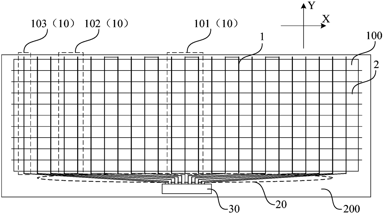
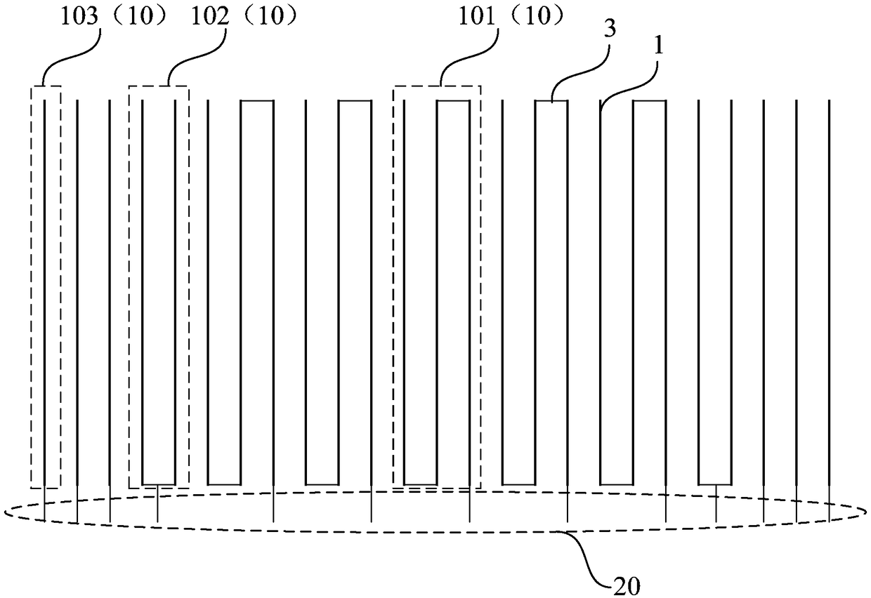
[0022] figure 1 A schematic structural diagram of an array substrate provided by an embodiment of the present invention; figure 2 A schematic diagram of data line distribution on an array substrate provided by an embodiment of the present invention. in, figure 2 The fan-out routing 20 is only drawn out as an example to illustrate the connection relationship between the fan-out routing 20 and the data line group 10 , not the actual arrangement of the fan-out routing 20 . Such as figure 1 and figure 2 As shown,


PUM


Abstract

The embodiment of the invention disclose an array substrate and an electronic paper display device. The array substrate includes a plurality of data lines arranged in the first direction and extendingin the second direction, and a plurality of scan lines arranged in the second direction and extending in the first direction, wherein the first direction intersects with the second direction; in thefirst direction, the data lines are continuously divided into multiple sets of data line groups, the data lines in the same data line group are electrically connected to each other, each set of the data line group is electrically connected to a driving circuit located in a non-display area through a fan-out line, the data line groups are arranged in the direction from the middle of a display areato the two sides, the number of the data lines in the latter set of the data line group is less than or equal to the number of the data lines in the previous set of the data line group, and the numberof the data lines in at least one data line group is smaller than the number of the data lines in the adjacent data line group. The array substrate improves the problem of data line resistance mismatch, and achieves a narrow frame design of an ultra-long electronic paper.

Description


Claims


Application Information

Patent Timeline
Owner SHANGHAI TIANMA MICRO ELECTRONICS CO LTD
Why Eureka
Try Eureka