Memristor based on bipolar transistor

A bipolar transistor and transistor technology, applied in the field of memristors, can solve the problems that the memristor devices cannot be commercialized, the technical realization is difficult, and the overall cost is high, and the effects of convenient circuit parameter adjustment, easy realization and low cost are achieved.

Pending Publication Date: 2019-09-06
南京邮电大学通达学院
View PDF0 Cites 0 Cited by
  • Summary
  • Abstract
  • Description
  • Claims
  • Application Information

AI Technical Summary

Benefits of technology

This patented technology allows for better control over electrical properties by creating an electronic device that uses only one type of material called amorphous silicon (aSi). By combining these materials together into a single layer or film, this method simplifies manufacturing processes while also reducing costs associated therewith. Additionally, it enables easier tuning parameters without requiring expensive components like passive elements such as inductance coils or resistance wires. Overall, this innovation improves performance and efficiency in memory devices used today.

Problems solved by technology

This patented describes how memory chips are used to create electronic circuits that have physical properties similar or identical with those found on other types of materials such as transistors. These techniques allow scientists to study these systems more efficiently while reducing their costs compared to traditional methods like silicon technology.

Method used


Image

  • Memristor based on bipolar transistor
  • Memristor based on bipolar transistor
  • Memristor based on bipolar transistor

Examples


Embodiment Construction

[0018] The specific implementation manners of the present invention will be further described in detail below in conjunction with the accompanying drawings.

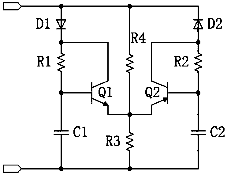
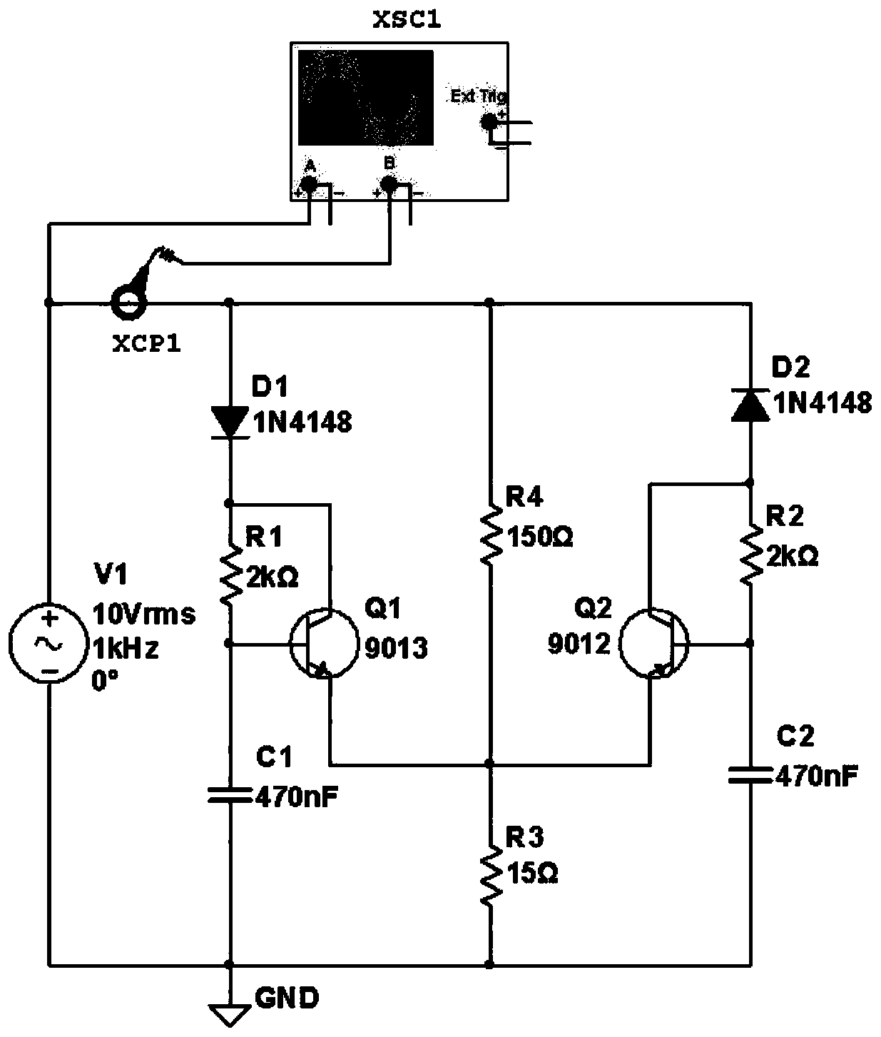
[0019] The present invention designs a memristor based on bipolar transistors, such as figure 1 As shown, in practical applications, it specifically includes a transistor Q1, a transistor Q2, a diode D1, a diode D2, a resistor R1, a resistor R2, a resistor R3, a resistor R4, a capacitor C1, and a capacitor C2.

[0020] Wherein, the anode of the diode D1 is respectively connected to one end of the resistor R4 and the cathode of the diode D2, and at the same time, the anode of the diode D1 is used as one of the external terminals of the memristor, and the cathode of the diode D1 is respectively connected to one end of the resistor R1 and the collector of the transistor Q1. electrode, the other end of the resistor R1 is respectively connected to the base of the transistor Q1 and one end of the capacitor C1, and the other end o


PUM


Abstract

The invention relates to a memristor based on a bipolar transistor. The memristor model overcomes the defects that a memristor model designed by adopting an active circuit chip is complex in structureand high in cost in the prior art. A brand-new design structure is adopted, the memristor is composed of the two transistors, the two diodes, the four resistors and the two capacitors, the memristorcircuit has the advantages of being simple in structure, easy to achieve, low in cost and convenient to adjust circuit parameters, and convenience is provided for researchers to research production and application of the memristor circuit.

Description


Claims


Application Information

Patent Timeline
Owner 南京邮电大学通达学院
Why Eureka
Try Eureka