DBC board layout method for reducing parasitic inductance of GaN HEMT power module packaging

A parasitic inductance and power module technology, applied in the field of DBC board layout to reduce the parasitic inductance of GaN HEMT power module packaging, can solve the problems of unreasonable thermal stress design, insufficient compatibility, troublesome heat dissipation, etc., to reduce chip performance degradation, The effect of avoiding mutual interference and reducing design cost

Inactive Publication Date: 2019-09-24
TONGHUI ELECTRONICS +1
View PDF6 Cites 2 Cited by
  • Summary
  • Abstract
  • Description
  • Claims
  • Application Information

AI Technical Summary

Benefits of technology

This patented technology improves how electronic devices work with higher voltage than previous designs without sacrificing their functionality or reliability due to increased heat generation compared to older designs. By leaving extra spaces on top instead of just relying solely upon added components, this allows more flexibility in terms of accommodating different types of circuits while maintaining good electrical characteristics such as efficiency and signal quality. Additionally, it simplifies the overall structure of the modules used within these systems, making them easier to manufacture at lower costs. Overall, this innovative solution enhances the performance and durability of electronics products.

Problems solved by technology

This patented describes how to efficiently arrange these components for use within an electronic device (GaN) chip package called GA). However, there are technical problem addressed by this method that can lead to poor performance or even failure when trying to meet specifications due to temperature differences between different parts inside the housing.

Method used


Image

  • DBC board layout method for reducing parasitic inductance of GaN HEMT power module packaging
  • DBC board layout method for reducing parasitic inductance of GaN HEMT power module packaging
  • DBC board layout method for reducing parasitic inductance of GaN HEMT power module packaging

Examples


Embodiment Construction

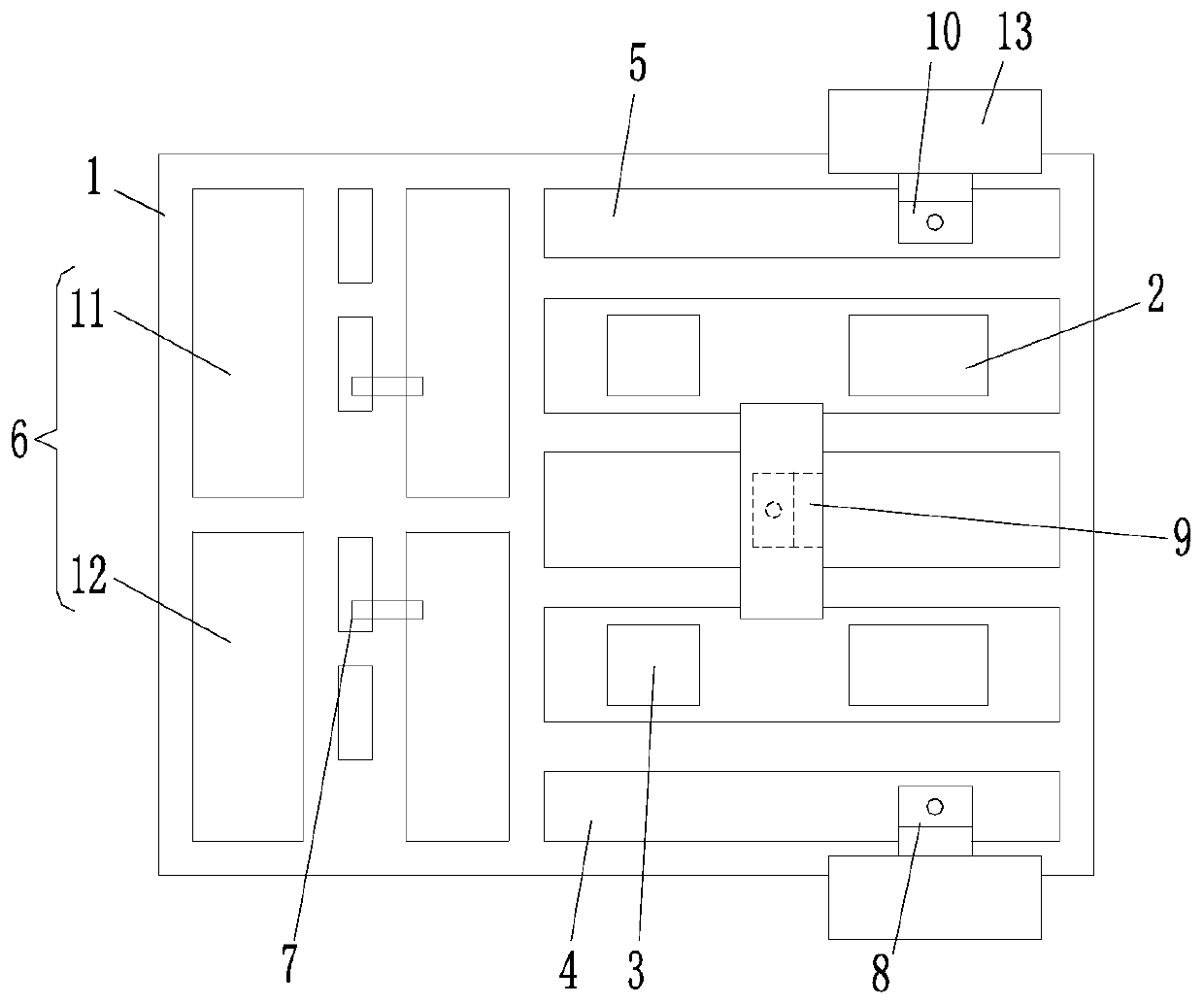
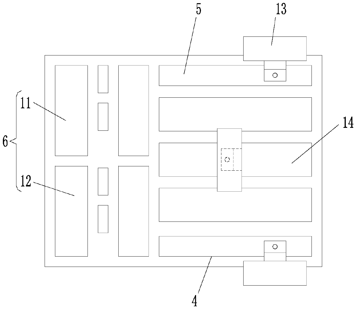
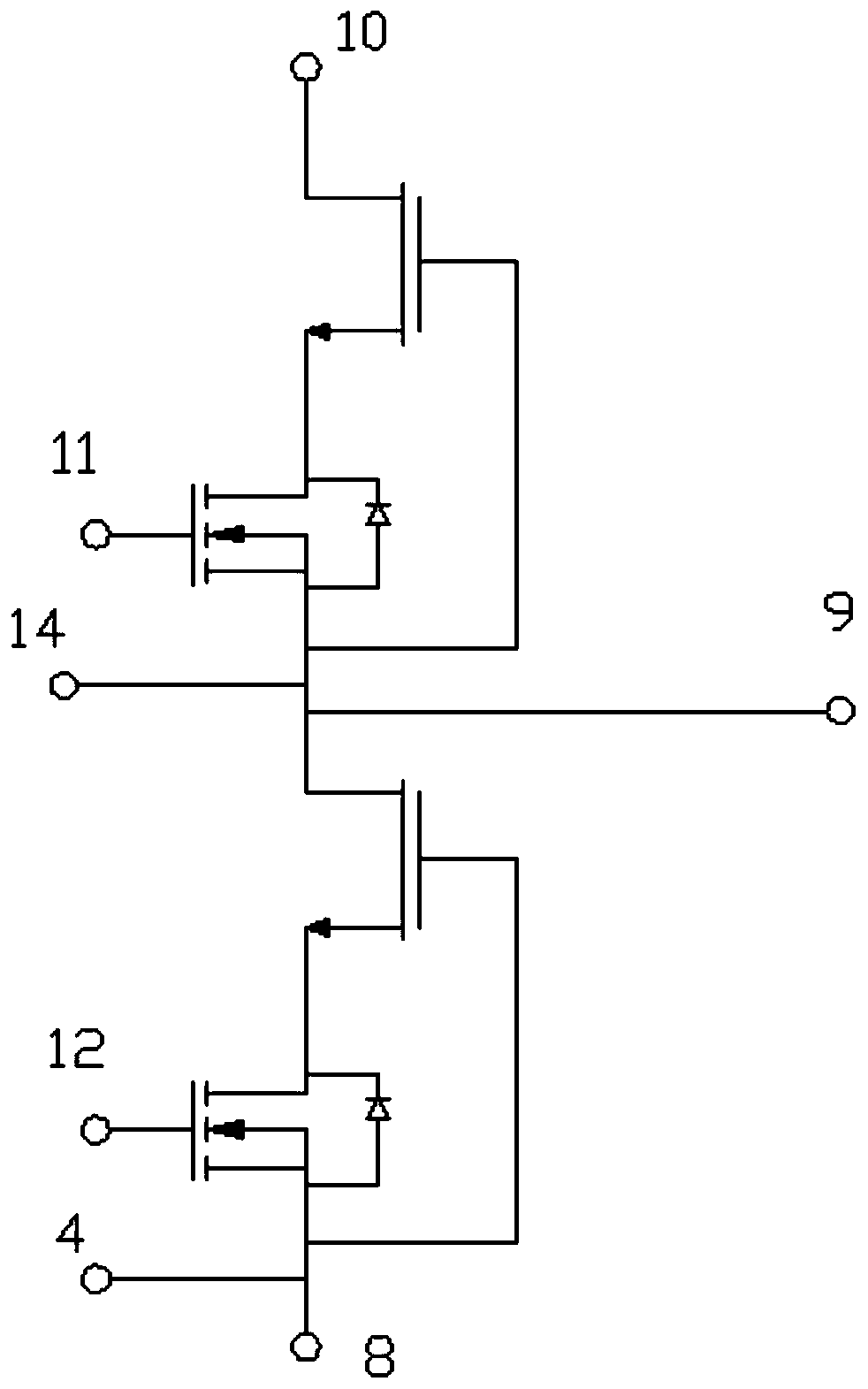
[0016] The invention relates to a DBC board layout method for reducing the parasitic inductance of GaN HEMT power module packaging, wherein the DBC board 1 is pasted with circuit design and layout components, and the components include a GaN chip 2, a MOS chip 3, a gate Resistor 7 and power terminal 13, said DBC board 1 includes source region 5, drain region 4, gate region 6, the key is that said GaN chip 2, MOS chip 3, gate resistor 7 and DBC The boards 1 are soldered by solder paste reflow, and the idle space left between the GaN chip 2 , the MOS chip 3 , the gate resistor 7 and the power terminal 13 is the copper clad on the DBC board 1 .

[0017] The present invention will be further described below with reference to the accompanying drawings and specific embodiments.

[0018] Specific examples, such as Figure 1-3 As shown, the gate region 6 is located at the side area of ​​the DBC board 1, the gate region 6 is distributed with a gate resistor 7, the GaN chip 2 and the MOS


PUM


Abstract

The invention relates to a DBC board layout method for reducing the parasitic inductance of GaN HEMT power module packaging, and belongs to the technical field of semiconductor packaging. The DBC board is pasted with components with circuit design layout, wherein the components include a GaN chip, an MOS chip, a gate resistor and a power terminal. The DBC board includes a source region, a drain region and a gate region, the GaN chip, the MOS chip, the gate resistor and the DBC board are welded by means of solder paste reflow, and the vacant space reserved among the GaN chip, the MOS chip, the gate resistor and the power terminal is clad copper on the DBC board. According to the invention, the DBC board is reasonably laid out, the parasitic inductance of the clad copper on the surface of the DBC board is improved, the loss caused by the overlarge parasitism of a GaN device in the packaging form at a high frequency is reduced, and the method for packaging the high-frequency GaN power module structure is realized.

Description


Claims


Application Information

Patent Timeline
Owner TONGHUI ELECTRONICS
Why Eureka
Try Eureka