Steep sloped vertical tunnel field-effect transistor
A field effect transistor and tunneling technology, applied in the field of tunneling field effect transistor devices
- Summary
- Abstract
- Description
- Claims
- Application Information
AI Technical Summary
Problems solved by technology
Method used
Image

Examples
Embodiment approach
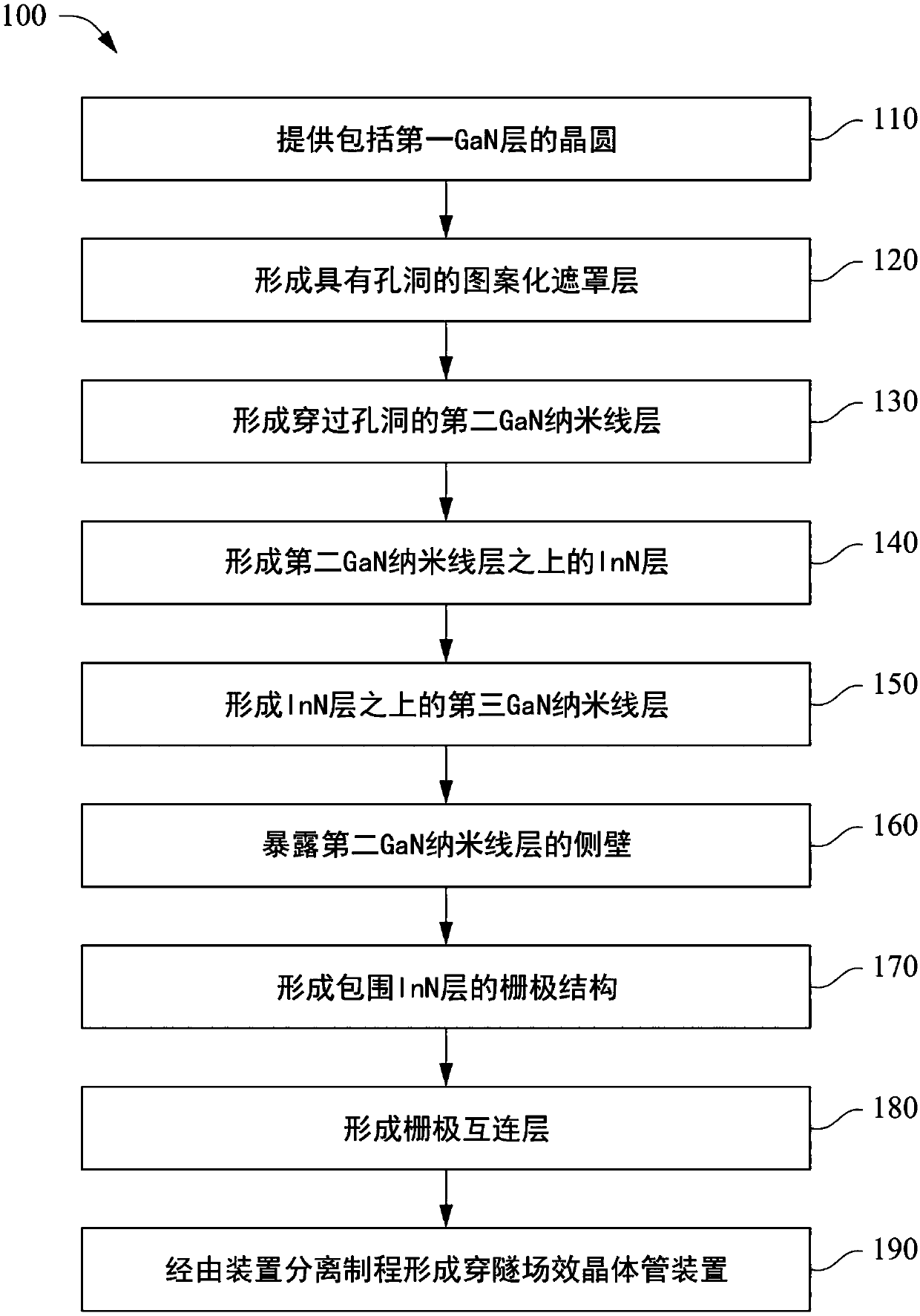
[0069] similar to Figure 2M As shown, according to the present disclosure, another exemplary embodiment of the Tunneling Field Effect Transistor device 400 includes: a first GaN layer 220 (GaN substrate) doped as N-type, and a mask layer 240 made of gallium nitride On the substrate 220 and including a hole 242, the second GaN nanowire layer 250 (the first nanowire source / drain region) covers the GaN substrate 220, extends upward through the hole 242 and is doped with the same N as the GaN substrate 220. type, InGaN or one or more layers of InN Intrinsic InN layer 270 (channel region), which covers the first nanowire source / drain region 250, third GaN nanowire layer 280 (second nanowire source / drain region) covers the channel region 270, and is doped to be P-type different from the GaN substrate 220 and the first nanowire source / drain region 250, and the gate structure (high-k dielectric layer 290 and metal The gate layer 300 ) is adjacent to the channel region 270 .
PUM
 Abstract
Description
Claims
Application Information
 - R&D Engineer
- R&D Manager
- IP Professional
- Industry Leading Data Capabilities
- Powerful AI technology
- Patent DNA Extraction
Browse by: Latest US Patents, China's latest patents, Technical Efficacy Thesaurus, Application Domain, Technology Topic.
© 2024 PatSnap. All rights reserved.Legal|Privacy policy|Modern Slavery Act Transparency Statement|Sitemap