Packaging structure and packaging method
A technology of packaging structure and chip structure, applied in the direction of electrical components, electrical solid devices, circuits, etc., can solve the problem of high interconnection cost, and achieve the effect of reducing packaging cost, neat appearance, and reducing area
- Summary
- Abstract
- Description
- Claims
- Application Information
AI Technical Summary
Benefits of technology
Problems solved by technology
Method used
Image

Examples
Embodiment 1
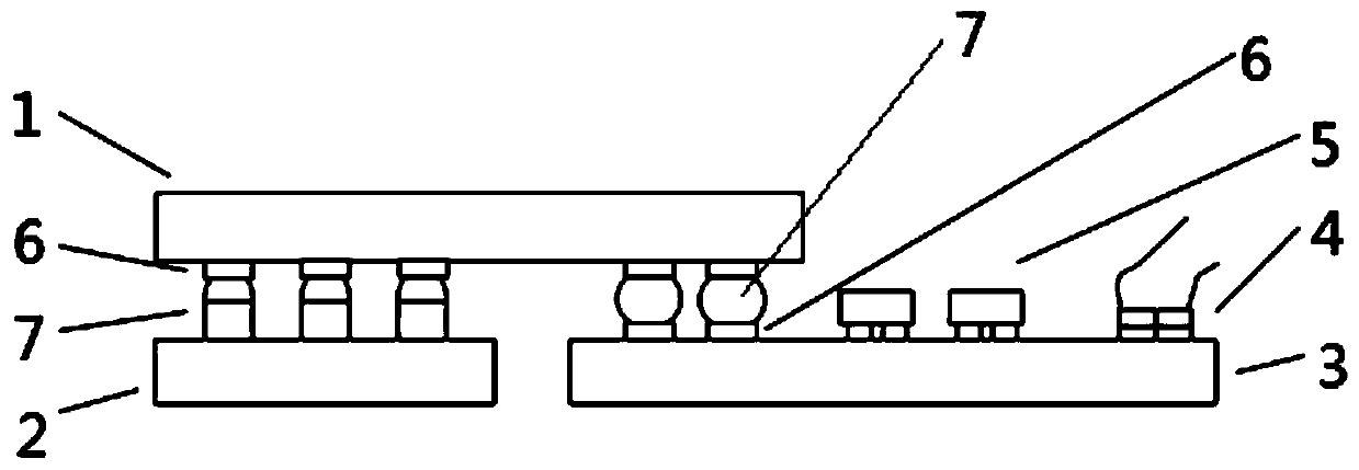
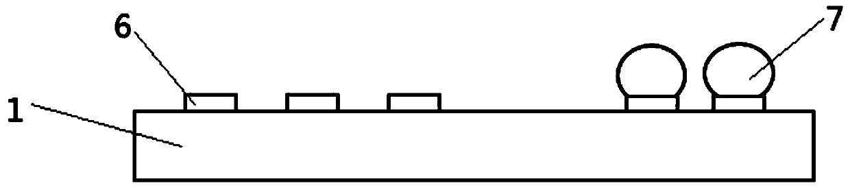
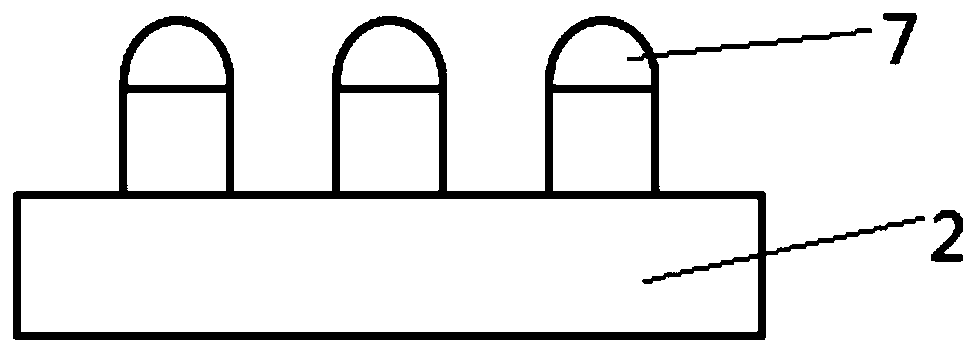
[0042] This embodiment provides a specific implementation of the packaging structure, which is mainly used to solve the interconnection problem between the silicon system module composed of the chip structure and the next-level system, such as Figure 1 to Figure 4 As shown, the packaging structure includes a first chip structure 1, a second chip structure 2, and a circuit board.
[0043] Wherein the second chip structure 2 is flip-chip connected on the first chip structure 1, the size of the second chip structure 2 is smaller than the size of the first chip structure 1, the circuit board is interconnected with the first chip structure 1, and the circuit board is connected to the second chip structure 1. The chip structure 2 is connected on the same surface of the first chip structure 1 , and the circuit board is provided with a connector 4 for connecting with the components to be connected. Wherein the connector 4 is used for connecting with the next-level system, the connector
Embodiment 2
[0055] This embodiment provides a packaging method, including the following steps:
[0056] A structure in which the second chip structure 2 is flip-chip connected to the first chip structure 1, the size of the second chip structure 2 is smaller than the size of the first chip structure 1, and the second chip structure 2 is flip-chip connected to the first chip structure 1 Such as Figure 5 shown;
[0057] The first chip structure 1 is flip-chip connected on the circuit board, and the circuit board is provided with a connector 4 for connecting with the parts to be connected. The structure after the first chip structure 1 is flip-chip connected on the circuit board is as follows: figure 1 shown.
[0058] By flip-chip connecting the second chip structure 2 to the first chip structure 1, the size of the second chip structure 2 is smaller than the size of the first chip structure 1, and the second chip structure 2 only occupies a part of the area of the first chip structure 1, O
PUM
 Abstract
Description
Claims
Application Information
 - R&D Engineer
- R&D Manager
- IP Professional
- Industry Leading Data Capabilities
- Powerful AI technology
- Patent DNA Extraction
Browse by: Latest US Patents, China's latest patents, Technical Efficacy Thesaurus, Application Domain, Technology Topic.
© 2024 PatSnap. All rights reserved.Legal|Privacy policy|Modern Slavery Act Transparency Statement|Sitemap