Chip FPC and manufacturing method thereof

A manufacturing method and chip technology, applied in the use/removal method of circuit masks, printed circuit manufacturing, printed circuits, etc., can solve the problems of increased production costs, waste of resources or energy, etc., to reduce weight and save production costs , to avoid the effect of wasting resources

Active Publication Date: 2020-12-18
RUISHENG NEW ENERGY DEV CHANGZHOU +1
View PDF11 Cites 0 Cited by
  • Summary
  • Abstract
  • Description
  • Claims
  • Application Information

AI Technical Summary

Problems solved by technology

However, for the convenience of subsequent positioning and operation, FPC typesetting usually leaves a waste area around it. There is no line area in the waste area, and the existence of wrinkles in the waste area does not affect the yield of the product. Therefore, the waste area does not need to be protected by a cover film, nor does it need to be laminated Carrying the film to enhance the strength, the material laminated in the waste area is actually a waste of resources or energy, resulting in an increase in production costs

Method used


Image

  • Chip FPC and manufacturing method thereof
  • Chip FPC and manufacturing method thereof
  • Chip FPC and manufacturing method thereof

Examples


Example Embodiment

[0033]The present invention will be further described below with reference to the drawings and embodiments.

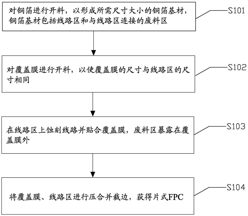
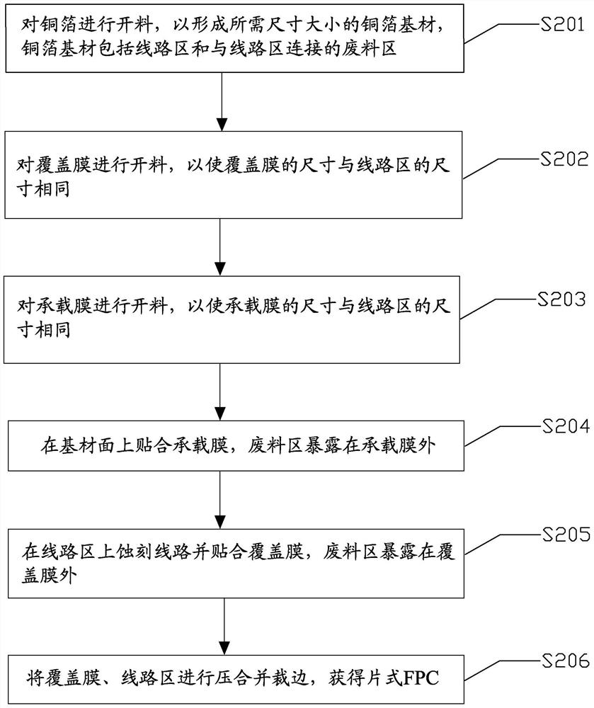
[0034]figure 1 It is a schematic flow chart of the manufacturing method of the chip FPC according to the first embodiment of the present invention. It should be noted that if there are substantially the same results, the method of the present invention does notfigure 1 The sequence of the processes shown is limited. Such asfigure 1 As shown, the method includes:

[0035]Step S101: cutting the copper foil to form a copper foil base material of a required size. The copper foil base material includes a circuit area and a waste area connected to the circuit area.

[0036]In step S101, the circuit area is used to place circuits and functional tool holes, and the waste area is used for subsequent positioning and operation. There is no need to place circuits and functional tool holes. Therefore, the waste area does not need to be covered with a film for protection and does not need to be attac


PUM

PropertyMeasurementUnit
Lengthaaaaaaaaaa

Abstract

The invention relates to the technical field of circuit board manufacturing, and provides a chip FPC and a manufacturing method thereof. The manufacturing method of the chip FPC comprises the steps ofcutting a copper foil to form a copper foil base material with the needed size, and the copper foil base material comprising a circuit area and a waste area connected with the circuit area; cutting acover film to enable the size of the cover film to be the same as the size of the circuit area; etching a circuit on the circuit area and attaching the cover film, wherein the waste area is exposed out of the cover film; and pressing and trimming the cover film and the circuit area to obtain the chip FPC. By means of the mode, the use amount of materials can be reduced, on one hand, the production cost is saved, resource waste is avoided, and on the other hand, the weight of the chip FPC is reduced.

Description


Claims


Application Information

Patent Timeline
Owner RUISHENG NEW ENERGY DEV CHANGZHOU
Why Eureka
Try Eureka