Conductive film

A technology of conductive film and conductive pillars, which is applied in the field of electronics, can solve the problems of insufficient area setting in the lead area, poor adaptability of the conductive layer, and limited functional areas, etc., and achieve the effects of reducing thickness, improving electrical conductivity, and improving stability

Active Publication Date: 2021-05-04
SHINE OPTOELECTRONICS KUNSHAN CO LTD
View PDF13 Cites 0 Cited by
  • Summary
  • Abstract
  • Description
  • Claims
  • Application Information

AI Technical Summary

Problems solved by technology

However, in some cases, such as the narrow border requirements of the touch screen, or when there are multiple conductive layers, not only the lower layer needs the lead area but also needs to make way for the upper layer lead area, resulting in insufficient area setting for the lead area, and the functional area is also limited. , resulting in poor adaptability of the conductive layer

Method used


Image

  • Conductive film
  • Conductive film
  • Conductive film

Examples


Example Embodiment

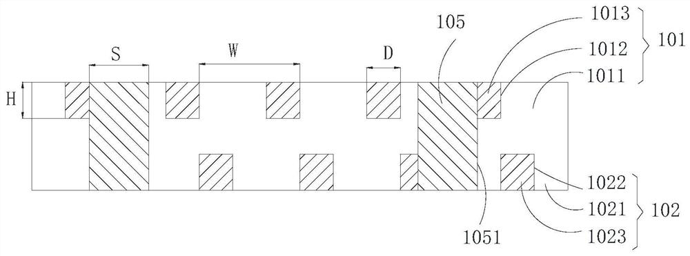
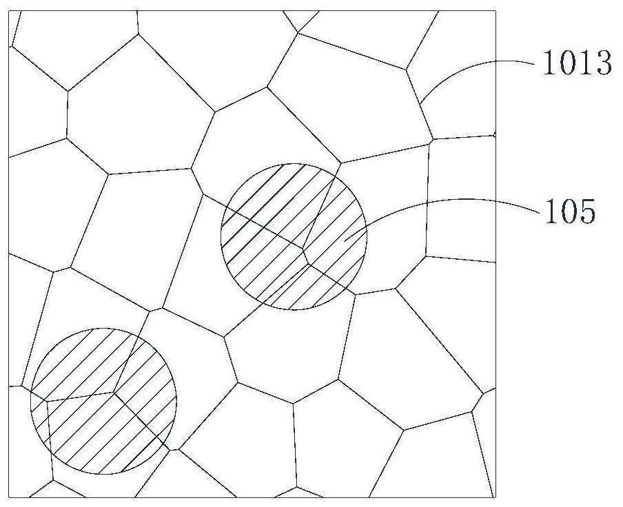
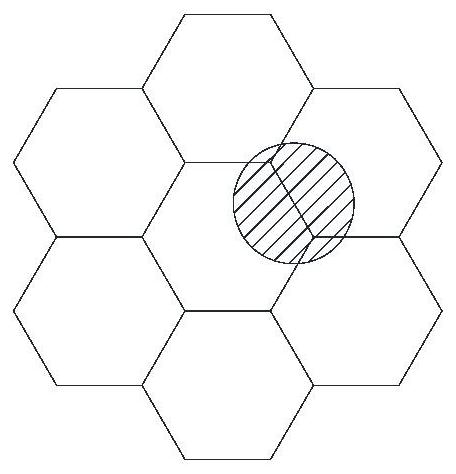
[0053] In order to facilitate understanding of the present invention, the present invention will be described more fully hereinafter with reference to the related drawings. The preferred embodiments of the invention are shown in the accompanying drawings. However, the present invention can be implemented in many different forms and is not limited to the embodiments described below. Rather, these embodiments are provided so that a thorough and complete understanding of the present disclosure is provided.

[0054] It should be noted that when an element is referred to as being "disposed on" another element, it can be directly on the other element or intervening elements may also be present. When an element is referred to as being "connected" to another element, it can be directly connected to the other element or intervening elements may also be present. The terms "vertical", "horizontal", "left", "right" and similar expressions used herein are for the purpose of illustration onl


PUM

PropertyMeasurementUnit
Widthaaaaaaaaaa
Widthaaaaaaaaaa
Thicknessaaaaaaaaaa

Abstract

The invention discloses a conductive film. The conductive film comprises N layers of conductive layers which are arranged in a stacked mode and a conductive column. Each conductive layer comprises a carrier and a conductive circuit arranged on the carrier; and N is greater than or equal to 2. The conductive column at least penetrates through one conductive layer and is electrically connected with the conductive circuits of at least two conductive layers. A lead of one conducting layer can be led to the other conducting layer through the conductive column; electric connection between two or more conducting layers can be achieved, the conductive film is not limited by the area of a lead area, a narrow frame is achieved, and wiring is convenient; and the plurality of conductive layers can be electrically connected, and the resistance of each conductive layer can be reduced, the shielding performance can be improved and the like only by arranging the lead on one conductive layer.

Description


Claims


Application Information

Patent Timeline
Owner SHINE OPTOELECTRONICS KUNSHAN CO LTD
Why Eureka
Try Eureka