SBG semiconductor laser device using electrode to realize sampling
A laser and semiconductor technology, applied in the field of optoelectronics, can solve the problems of increasing manufacturing cost, increasing sampling pattern lithography process, complex processing, etc., to achieve the effect of reducing complexity and manufacturing cost, improving threshold performance and quantum conversion efficiency
- Summary
- Abstract
- Description
- Claims
- Application Information
AI Technical Summary
Problems solved by technology
Method used
Image

Examples
Embodiment 1
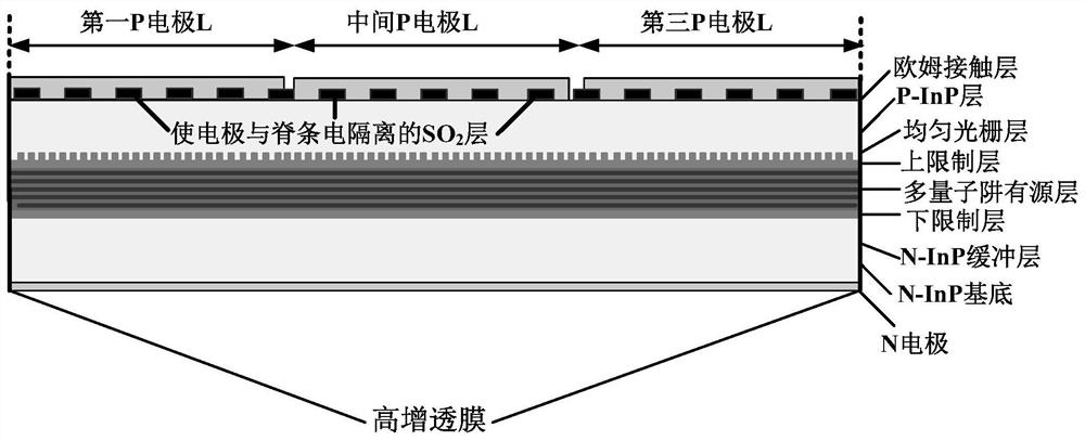
[0022] The present embodiment provides a kind of SBG semiconductor laser device that realizes sampling with three electrodes, as figure 2 As shown, the grating along the laser cavity is a uniform grating, which has three electrically isolated electrodes, and the center of the sampling pattern formed by the middle electrode and the conductive area between the ridges can be a uniform sampling pattern with or without equivalent phase shift. Both ends of the laser are coated with high anti-reflection coating.
[0023] The implementation principle of the fine adjustment of the lasing wavelength of the SBG semiconductor laser device in this embodiment is as follows:
[0024] we take figure 2 As an example to illustrate, for the sake of simplicity, let the lengths of the electrodes at both ends and the middle electrode be L R = L, L P =L, then when the electrodes at both ends of the laser are injected with the same current density and the middle electrode is injected with different
Embodiment 2
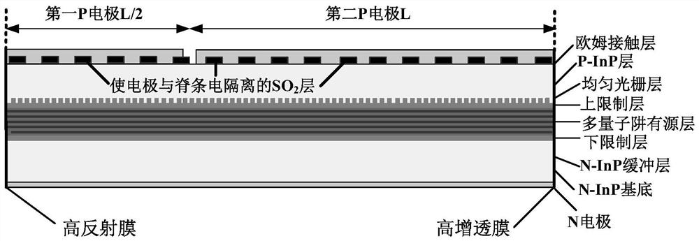
[0028] The present embodiment provides a kind of SBG semiconductor laser device that realizes sampling with two electrodes, as image 3 As shown, the grating along the laser cavity is a uniform grating, which has two electrically isolated electrodes, and the two ends of the laser are coated with high reflection film and high anti-reflection film respectively.
[0029] The implementation principle of the fine adjustment of the lasing wavelength of the SBG semiconductor laser device in this embodiment is as follows:
[0030] we take figure 2 As an example to explain, for the sake of simplicity, the lengths of the end electrodes coated with high anti-reflection coating and high reflection coating are respectively L P =L, then when the two electrodes of the laser are injected with different current densities, the effective refractive index n of the laser cavity under the two electrodes of the laser R and n P will be different, and also in the lasing channel will obtain a distri
PUM
 Abstract
Description
Claims
Application Information
 - R&D Engineer
- R&D Manager
- IP Professional
- Industry Leading Data Capabilities
- Powerful AI technology
- Patent DNA Extraction
Browse by: Latest US Patents, China's latest patents, Technical Efficacy Thesaurus, Application Domain, Technology Topic.
© 2024 PatSnap. All rights reserved.Legal|Privacy policy|Modern Slavery Act Transparency Statement|Sitemap