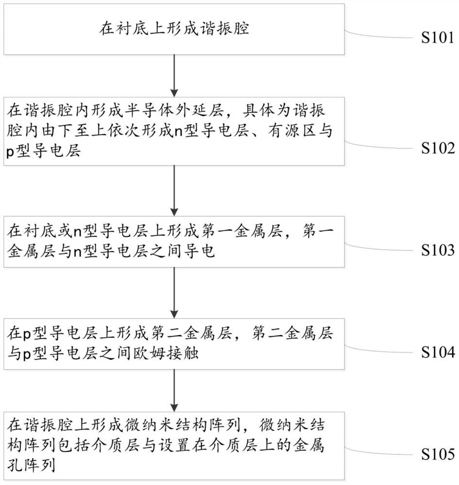
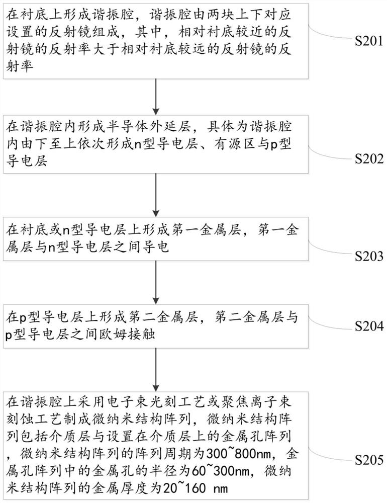
RCLED-based sensor and manufacturing method thereof
- Summary
- Abstract
- Description
- Claims
- Application Information
AI Technical Summary
Benefits of technology
Problems solved by technology
Method used
Image

Examples
example 1
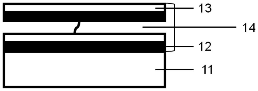
[0092] This example takes a GaAs-based RCLED with a luminous center wavelength of 650nm as an example to provide a manufacturing method for an RCLED-based sensor, including the following steps:
[0093] S301: Reference image 3 , using metal organic chemical vapor deposition (MOCVD) or molecular beam epitaxy (MBE) method to set TiO on n-type GaAs substrate 11 2 High refractive index layer 12 and MgF 2 Low refractive index layer 13, TiO 2 High refractive index layer 12 and MgF 2 The low refractive index layer 13 forms a bottom distributed Lagg reflector 14 whose sum of layers is 60 layers by setting the number of material layers, wherein the central reflection wavelength of the bottom distributed Lagg reflector 14 is 650nm, and TiO 2 The refractive index n1=2.45 of the high refractive index layer 12, then its physical thickness is 66.3nm; MgF 2 The low refractive index layer 13 has a refractive index n2=1.37, so its physical thickness is 118.6 nm;
[0094] S302: Reference F
example 2
[0103] For easy understanding, please refer to Figure 10 , this example takes a GaN-based semiconductor material with a luminescence peak of 570nm as an example to provide a manufacturing method for an RCLED-based sensor, including the following steps:
[0104] S401: Arranging an AlGaN high refractive index layer 82 and a GaN low refractive index layer 83 on a sapphire substrate 81 by metal organic chemical vapor deposition (MOCVD) or molecular beam epitaxy (MBE), the AlGaN high refractive index layer 82 and the GaN low refractive index layer The ratio layer 83 forms a bottom distributed Lager reflector 84 with a sum of layers of 40 layers by setting the number of material layers, wherein the central reflection wavelength of the bottom distributed Lager reflector 84 is 500nm;
[0105] S402: Forming a GaN-based semiconductor epitaxial layer on the bottom distributed Lager mirror 84, the GaN-based semiconductor epitaxial layer is provided with an n-type GaN epitaxial layer 85, a q
PUM
| Property | Measurement | Unit |
|---|---|---|
| Radius | aaaaa | aaaaa |
| Physical thickness | aaaaa | aaaaa |
| Physical thickness | aaaaa | aaaaa |
Abstract
Description
Claims
Application Information
 - R&D Engineer
- R&D Manager
- IP Professional
- Industry Leading Data Capabilities
- Powerful AI technology
- Patent DNA Extraction
Browse by: Latest US Patents, China's latest patents, Technical Efficacy Thesaurus, Application Domain, Technology Topic.
© 2024 PatSnap. All rights reserved.Legal|Privacy policy|Modern Slavery Act Transparency Statement|Sitemap