Display panel and display device

A display panel and display area technology, applied to static indicators, instruments, etc., can solve the problems of large data signal potential differences, high power consumption of source drive circuits, etc., and achieve the effect of low power consumption

Pending Publication Date: 2022-06-07
BOE TECH GRP CO LTD +1
View PDF0 Cites 0 Cited by
  • Summary
  • Abstract
  • Description
  • Claims
  • Application Information

AI Technical Summary

Benefits of technology

The present technology relates to an improved method or system for controlling how much electricity goes into displaying devices (such as displays) while maintaining their effectiveness at all times without overloading them too heavily. This means they will have less energy usage compared to traditional methods like turning off lights when there's no activity on top.

Problems solved by technology

This patented method divides an entire surface or sectional part (the upper) of a display panel into two parts - one where regular displays appear while another has sensor devices placed there. By doing it over time, these sensor devices will work together more efficiently when displaying images. However, if some specific regions have certain properties like being darker during image presentation compared to other sections they may also show up too much energy usage due to their own characteristics such as resolutions and color depth levels.

Method used


Image

  • Display panel and display device
  • Display panel and display device
  • Display panel and display device

Examples


Embodiment Construction

[0055] In order to make the objectives, technical solutions and advantages of the present disclosure clearer, the embodiments of the present disclosure will be further described in detail below with reference to the accompanying drawings.

[0056] The transistors used in all the embodiments of the present disclosure may be thin film transistors, field effect transistors, or other devices with the same characteristics, and the transistors used in the embodiments of the present disclosure are mainly switching transistors according to their functions in the circuit. Since the source and drain of the switching transistor used here are symmetrical, the source and drain are interchangeable. In the embodiments of the present disclosure, the source electrode is referred to as the first electrode and the drain electrode is referred to as the second electrode; or, the drain electrode is referred to as the first electrode and the source electrode is referred to as the second electrode. Acco


PUM


Abstract

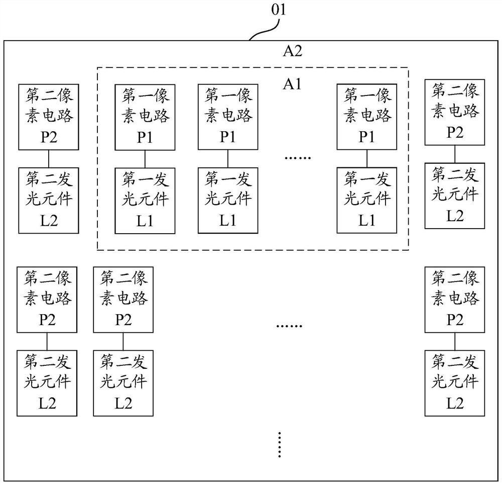
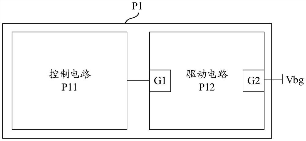
The invention provides a display panel and a display device, and belongs to the technical field of display. In the display panel, each of a first pixel circuit located in a first display area and a second pixel circuit located in a second display area comprises a driving circuit with two grid electrodes, and one grid electrode is used for receiving a power supply signal. The potential of the power supply signal received by the grid electrode of the driving circuit in the first pixel circuit is different from that of the power supply signal received by the grid electrode of the driving circuit in the second pixel circuit. Therefore, the independent control of the characteristics of the transistor included in the driving circuit in the first pixel circuit and the characteristics of the transistor included in the driving circuit in the second pixel circuit is realized. Therefore, in different scenes of the first pixel circuit and the second pixel circuit, the source driving circuit transmits data signals with small potential difference to the two pixel circuits, so that two light-emitting elements driven by the two pixel circuits have the same light-emitting brightness. Correspondingly, the working power consumption of the source electrode driving circuit is low.

Description


Claims


Application Information

Patent Timeline
Owner BOE TECH GRP CO LTD
Why Eureka
Try Eureka