Method for making cathode structure of field emitting display

A technology of cathode structure and manufacturing method, which is applied in the direction of electroluminescent light source, lighting device, light source, etc., can solve the problems of uneven electric field effect, uneven current density of electron beam, difficult to compact structure, etc., and achieve uniformity of brightness , Improve the uniformity of the electric field and reduce the production accuracy

Inactive Publication Date: 2006-01-11
TECO NANOTECH CO LTD
View PDF0 Cites 0 Cited by
  • Summary
  • Abstract
  • Description
  • Claims
  • Application Information

AI Technical Summary

Benefits of technology

This patented technology allows for better control over how well an emitter made from a single type of conductive polymer works when it comes into contact with another metal plate called target plates during assembling processes. By creating this new design, the device becomes lighter and thinner than previous designs while maintaining their performance level. Additionally, by improving the accuracy at which two layers are formed on top of one other, we aimed towards achieving even electrical fields within the assembled devices without any unwanted side effects such as scattered radiation. Overall, these improvements lead to higher-quality images being produced through the use of this novel approach.

Problems solved by technology

This patented technical problem addressed in the patents relates to improving the performance and quality of electronic displays that require high voltages for operation. Current techniques like ionization discharge have limitations in terms of producing uniform films on large substrate surfaces while also requiring multiple steps during fabrication processes. These issues lead to variations between different materials and reduced productivity rates.

Method used


Image

  • Method for making cathode structure of field emitting display
  • Method for making cathode structure of field emitting display
  • Method for making cathode structure of field emitting display

Examples


Embodiment Construction

[0027] Relevant technical content and detailed description of the present invention, now cooperate accompanying drawing to explain as follows:

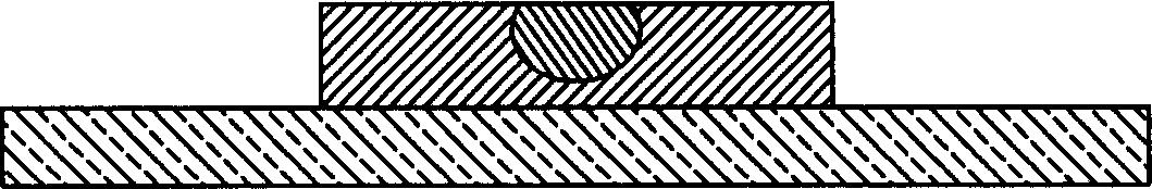
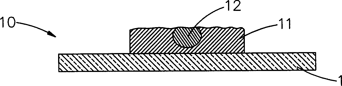
[0028] figure 2 , image 3 It is a schematic diagram of the fabrication process and a schematic diagram of the cathode structure of the cathode structure of the field emission display of the present invention. Such as figure 2 , image 3 As shown, the method for manufacturing the cathode structure of the field emission display of the present invention is mainly to use grinding technology to level the surface of the electrode layer of the cathode structure after the cathode structure of the field emission display is manufactured, so that the surface flatness of the electrode layer is improved, and It is easier to make and can reduce the production cost.

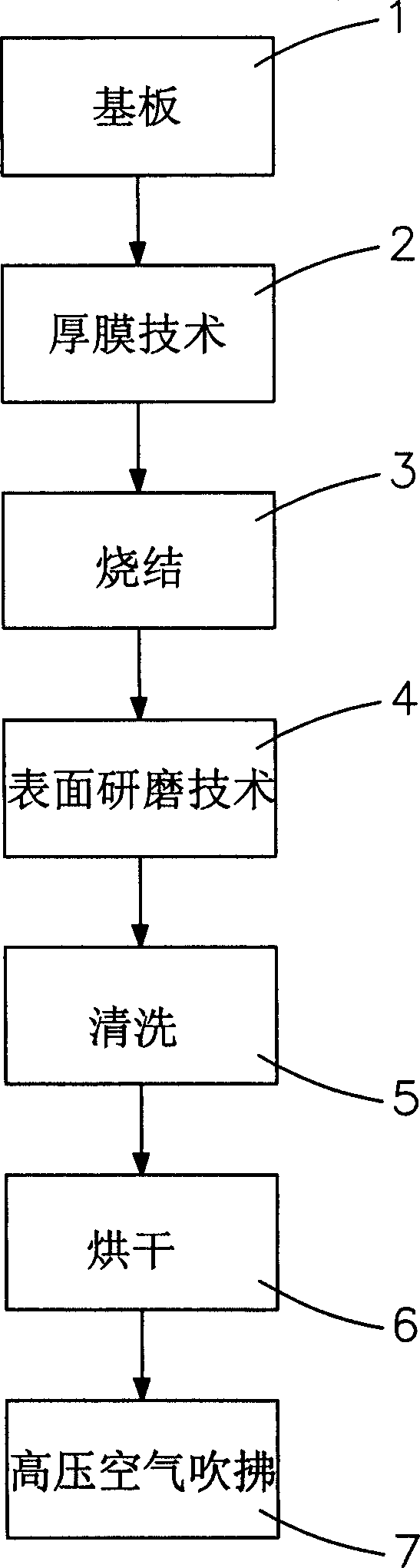
[0029] When making the cathode structure, take a substrate 1 first, and the substrate 1 is made of glass material;

[0030] The first and second electrode layers 11 and 12 are mad


PUM

PropertyMeasurementUnit
Particle sizeaaaaaaaaaa

Abstract

This invention relates to a cathode structure process method for a field emit display, which forms a first and second electrode layers on a base plate made of silver ink and nm carbon tube material applying thick film technology and sinters the silver ink, after that, the silver ink and the first, second electrode layer surfaces are ground, the thickness error after grinding can be controlled at less than 0.1mum and the flatness of the first and second electrode surfaces is increased.

Description


Claims


Application Information

Patent Timeline
Owner TECO NANOTECH CO LTD
Why Eureka
Try Eureka