Plasma display panel

a technology of display panels and plasma, applied in gas discharge vessels/containers, electric discharge tubes, gas-filled discharge tubes, etc., can solve the problems of unable to provide excellent screen displays, unable to withstand voltage disadvantages, exfoliation, cracking, etc., and achieve excellent screen displays. , the effect of reducing the occurrence of disadvantages such as cracking and chipping

Inactive Publication Date: 2005-11-03
PANASONIC CORP
View PDF5 Cites 0 Cited by
  • Summary
  • Abstract
  • Description
  • Claims
  • Application Information

AI Technical Summary

Benefits of technology

The invention relates to improving the quality of displays made from plasmas that use less expensive materials for better performance compared to traditional methods like liquid crystal or cathode ray tube (CRT).

Problems solved by technology

This patented technical solution described in the patents relates to improving the performance (performance) and lifespan of plasma Display Panels due to issues like insufficient resistance against voltages while maintaining good image clarity and resolution capabilities.

Method used


Image

  • Plasma display panel
  • Plasma display panel
  • Plasma display panel

Examples


Embodiment Construction

[0017] A plasma display panel according to an embodiment of the present invention will be detailed as follows with reference to accompanying drawings.

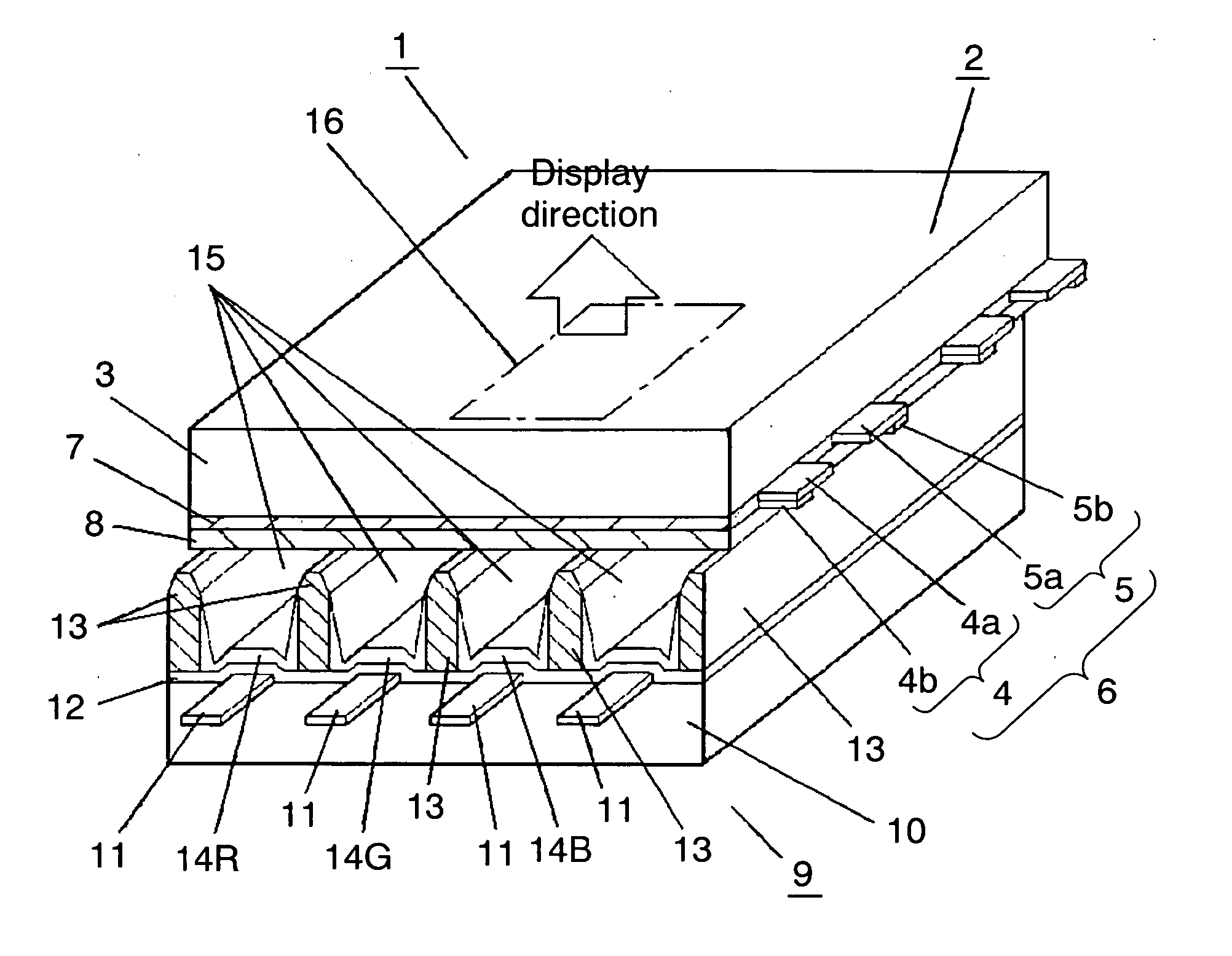
[0018]FIG. 1 is a perspective cross sectional view showing a schematic structure of the plasma display panel according to the embodiment of the present invention.

[0019] As shown in FIG. 1, PDP 1 is formed of front plate 2 and back plate 9. Front plate 2 includes front substrate 3 made of a transparent and insulating glass substrate or the like; display electrode 6 which is provided on front substrate 3 and which consists of scan electrode 4 and sustain electrode 5; first dielectric layer 7 which covers display electrode 6; and protective layer 8 which is made of MgO film and covers first dielectric layer 7. Scan electrode 4 and sustain electrode 5 are formed by stacking bus electrodes 4b and 5b made from metallic material onto transparent electrodes 4a and 5a, respectively, for the purpose of securing light transmission properties and r


PUM


Abstract

A plasma display panel does not cause disadvantages such as exfoliating or chipping in dielectric layers. The plasma display panel includes a first dielectric layer (7) for covering a display electrode which is formed on a front substrate (3) and which consists of a scan electrode and a sustain electrode, and a second dielectric layer for covering a data electrode formed on a back substrate, and the peripheries of the first dielectric layer (7) and/or the second dielectric layer have a radius of curvature of other than 0.

Description


Claims


Application Information

Patent Timeline
Owner PANASONIC CORP
Why Eureka
Try Eureka