Thin film transistor and method of fabricating the same

a thin film transistor and film technology, applied in the direction of transistors, semiconductor devices, electrical equipment, etc., can solve the problems of easy transformation, short processing time, and damage to the silicon layer, and achieve excellent characteristics

Active Publication Date: 2006-02-16
SAMSUNG DISPLAY CO LTD
View PDF2 Cites 44 Cited by
  • Summary
  • Abstract
  • Description
  • Claims
  • Application Information

AI Technical Summary

Benefits of technology

The technical effect described this patented technology allows for better performance of thin films made from materials like amorphously-silicone or metals with high melting points such as platinum. This results in improved device properties over existing methods due to lesser amounts of expensive material being used compared to traditional techniques.

Problems solved by technology

This patented technical problem addressed in this patents relates to improving the efficiency of producing displays with improved performance characteristics without requiring expensive equipment like vacuum tube devices. Current methods involve forming layers from different materials onto a special type of substrate called a “glass”, but these techniques have drawbacks including longer processes times due to exposing it to higher temperatures while maintaining good interfaces between the various components involved.

Method used


Image

  • Thin film transistor and method of fabricating the same
  • Thin film transistor and method of fabricating the same
  • Thin film transistor and method of fabricating the same

Examples


Embodiment Construction

[0018] The present invention will now be described more fully hereinafter with reference to the accompanying drawings, in which preferred embodiments of the invention are shown. This invention may, however, be embodied in different forms and should not be construed as limited to the embodiments set forth herein. Rather, these embodiments are provided so that this disclosure will be thorough and complete, and will fully convey the scope of the invention to those skilled in the art. In the drawings, the thickness of layers and regions are exaggerated for clarity. Like numbers refer to like elements throughout the specification.

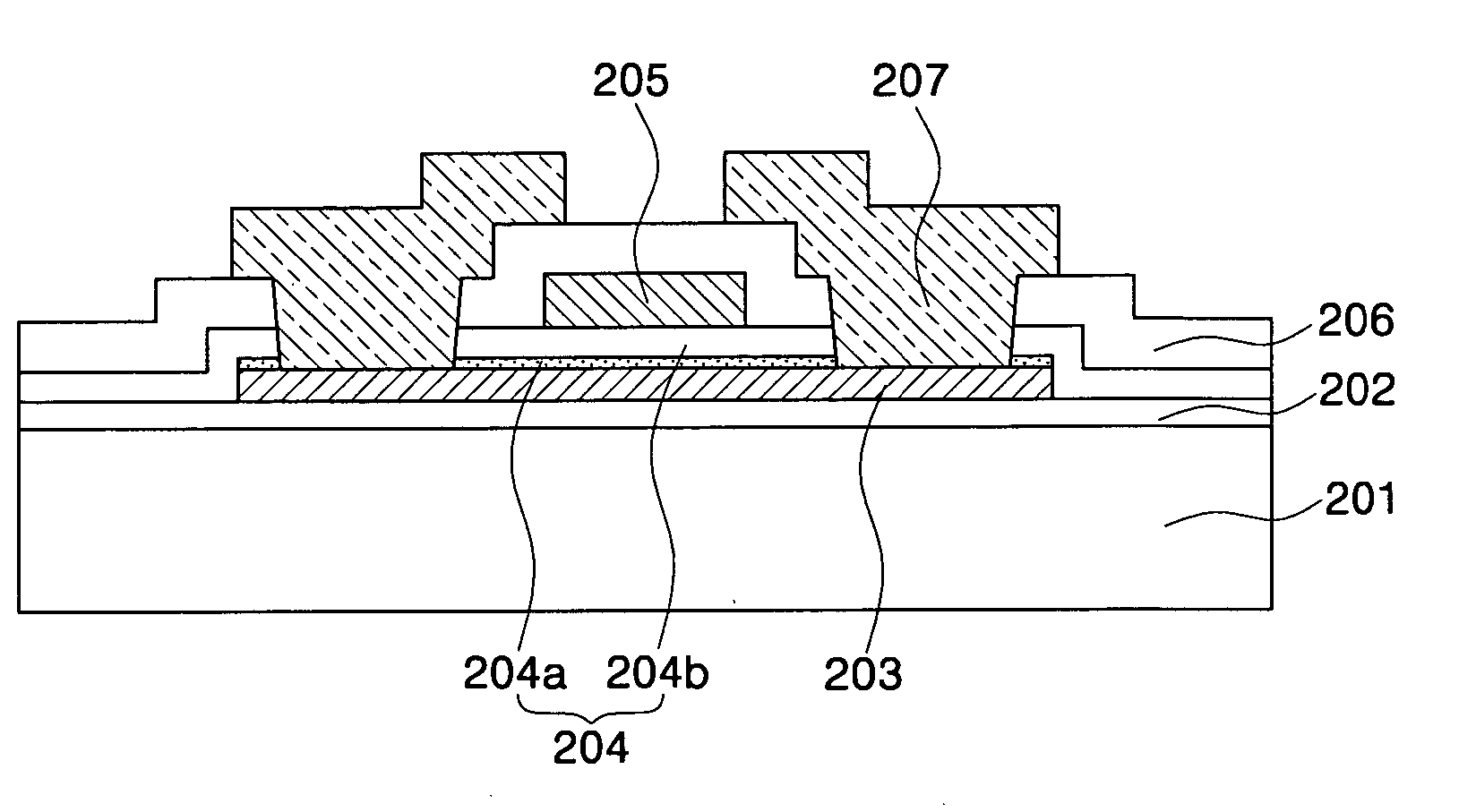
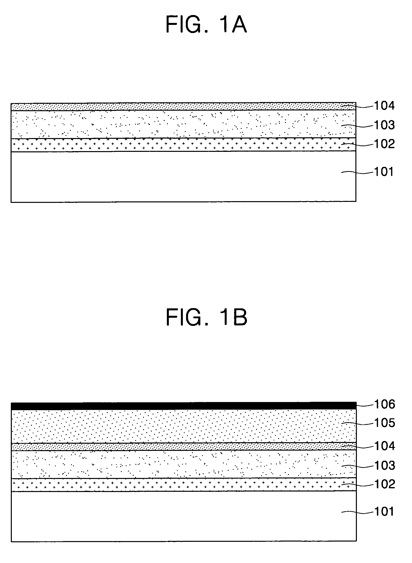
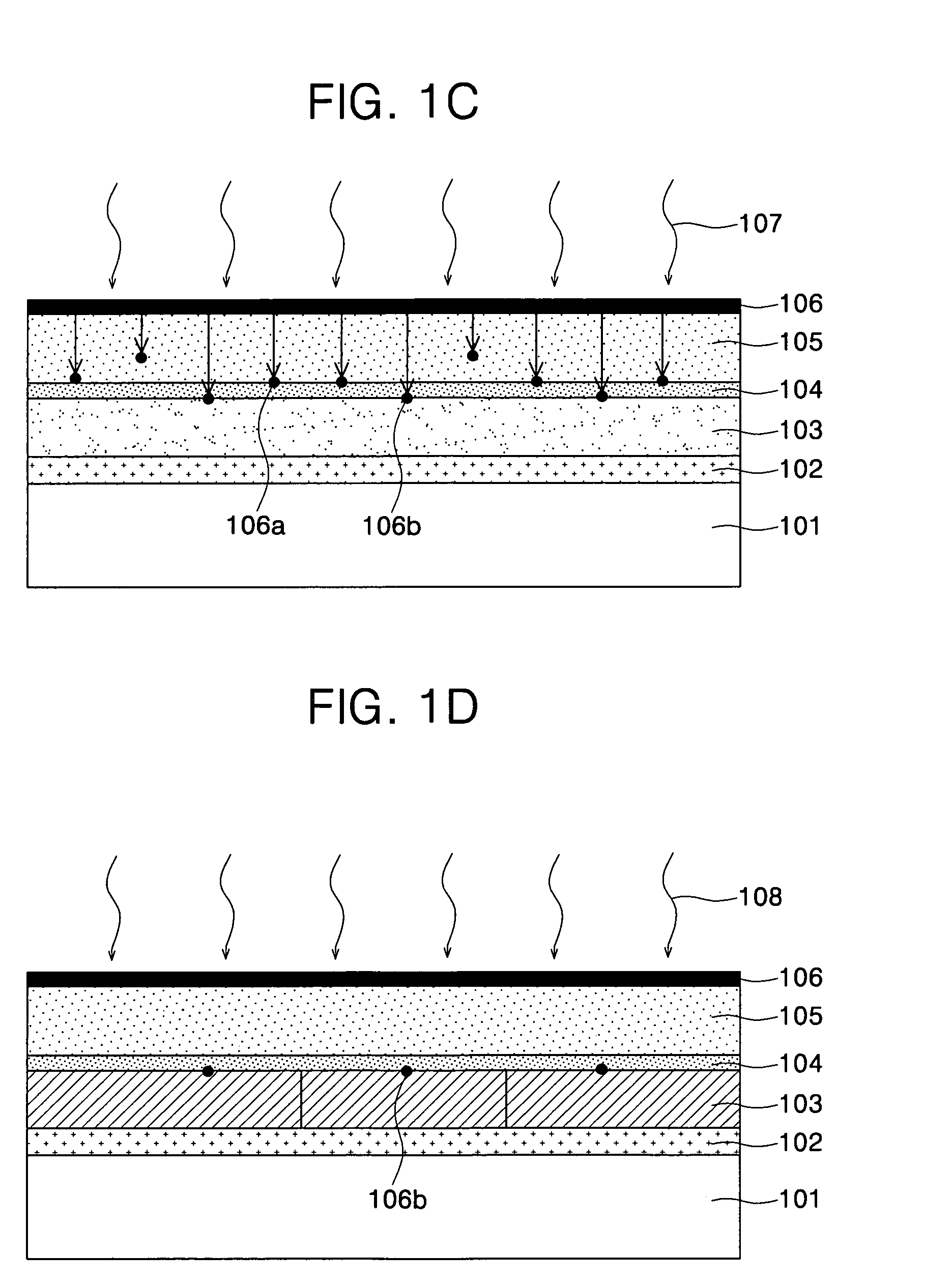
[0019]FIGS. 1a to 1d are cross-sectional views illustrating a crystallization process according to the present invention.

[0020] First, FIG. 1a is a cross-sectional view illustrating a process of sequentially forming a buffer layer, an amorphous silicon layer and a filtering oxide layer on a substrate. As shown in FIG. 1a, a buffer layer 102 is formed on an insula


PUM


Abstract

The present invention discloses a thin film transistor and a method of fabricating the same. The thin film transistor includes an insulating substrate; and a semiconductor layer, a gate insulating layer, a gate electrode, an interlayer insulator, and a source/drain electrode which are formed on the substrate, wherein the gate insulating layer is formed of a filtering oxide layer having a thickness of 1 to 20 Å.

Description


Claims


Application Information

Patent Timeline
Owner SAMSUNG DISPLAY CO LTD
Why Eureka
Try Eureka