Capillary underfill and mold encapsulation method and apparatus

Active Publication Date: 2006-09-28
INTEL CORP
View PDF10 Cites 5 Cited by
  • Summary
  • Abstract
  • Description
  • Claims
  • Application Information

AI Technical Summary

Problems solved by technology

The high clamping force and the high transfer pressure causes the ILD to crack during the MUF process.
Cracks in the ILD result in failures of the flip ch

Method used


Image

  • Capillary underfill and mold encapsulation method and apparatus
  • Capillary underfill and mold encapsulation method and apparatus
  • Capillary underfill and mold encapsulation method and apparatus

Examples


Embodiment Construction

[0022] In the following detailed description, reference is made to the accompanying drawings, which are not necessarily to scale, which form a part hereof, and in which is shown, by way of illustration, specific embodiments in which the apparatus and methods can be practiced. These embodiments are described in sufficient detail to enable those skilled in the art to practice them, and it is to be understood that the embodiments can be combined, or that other embodiments can be utilized and that procedural changes can be made without departing from the spirit and scope of the present invention. The following detailed description is, therefore, not to be taken in a limiting sense, and the scope is defined by the appended claims and their equivalents. In the drawings, like numerals describe substantially similar components throughout the several views.

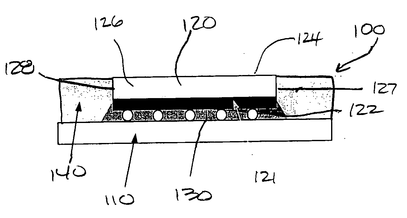
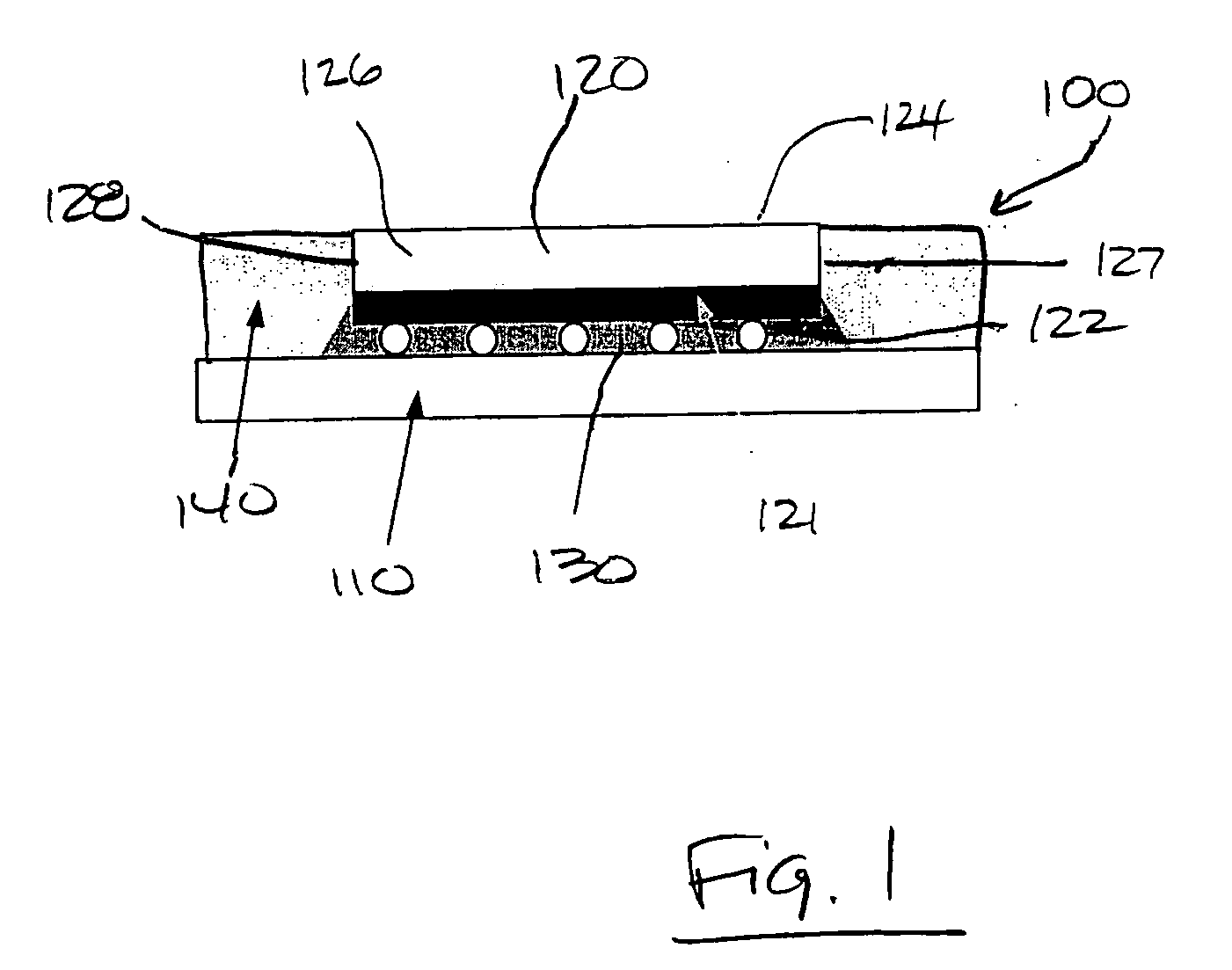
[0023]FIG. 1 is schematic cutaway view of a semiconductor package 100, according to an embodiment of the invention. The semiconductor packa


PUM


Abstract

A method of packaging a die includes attaching the die to a substrate; underfilling the space between the die and the substrate with a first material, and placing a second material in contact with at least a portion of the die and the substrate after underfilling the space between the die and substrate with the first material. A system includes a semiconductor package having a substrate, a die attached to the substrate, an underfill material positioned between the die and the substrate, and a molding material in contact with at least a portion of the substrate and the die. A heat sink is also in thermal contact with the semiconductor package.

Description


Claims


Application Information

Patent Timeline
Owner INTEL CORP
Why Eureka
Try Eureka