Semiconductor memory and operation method for same
a technology of semiconductors and memory, applied in the field of semiconductor memory, can solve the problems reducing the resistance of the bit line, and achieve the effects of shortening the precharge operation time, shortening the access cycle time, and reducing the current consumption
- Summary
- Abstract
- Description
- Claims
- Application Information
AI Technical Summary
Benefits of technology
Problems solved by technology
Method used
Image

Examples
first embodiment
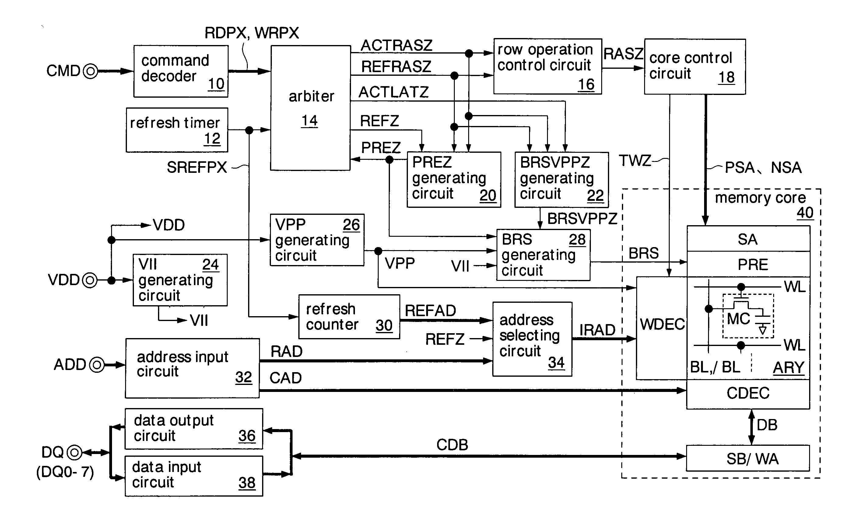
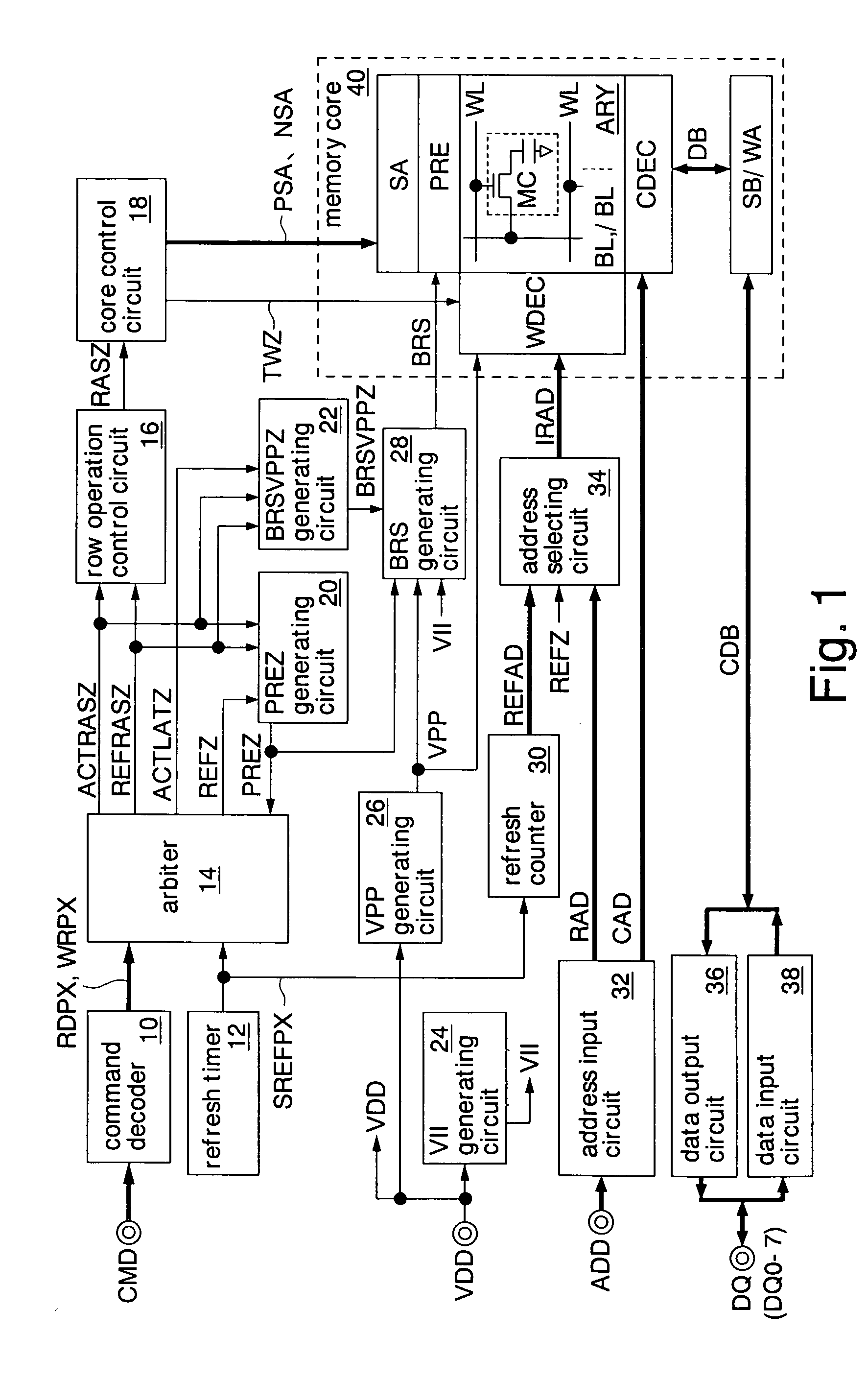
[0039]FIG. 1 shows the semiconductor memory of the invention. The semiconductor memory is formed as a pseudo-SRAM having a DRAM memory cell (i.e., a dynamic memory cell) and an interface of SRAM. The pseudo-SRAM executes the refresh operation periodically in the chip without any refresh command from the outside, and retains the data written in the memory cell. This pseudo-SRAM is employed in a work memory to be mounted on a mobile phone, for example.
[0040] The pseudo-SRAM includes a command decoder 10, a refresh timer 12, an arbiter 14, a row operation control circuit 16, a core control circuit 18, a PREZ generating circuit 20, a BRSVPPZ generating circuit 22 (or a switch control circuit), a VII generating circuit 24 (or an internal supply voltage generating circuit), a VPP generating circuit 26 (or a boost voltage generating circuit), a BRS generating circuit 28, a refresh counter 30, an address input circuit 32, an address selecting circuit 34, a data output circuit 36, a data input
second embodiment
[0110]FIG. 12 shows an operation example of the pseudo-SRAM in the In this example, the refresh request SREFPX occurs (for an access period) for the access requests RDPX and WRPX (or the read command RD and the write command WR), and only the refresh request SREFPX then occurs periodically (for a standby period) for the standby period of no access request RDPX and WRPX.
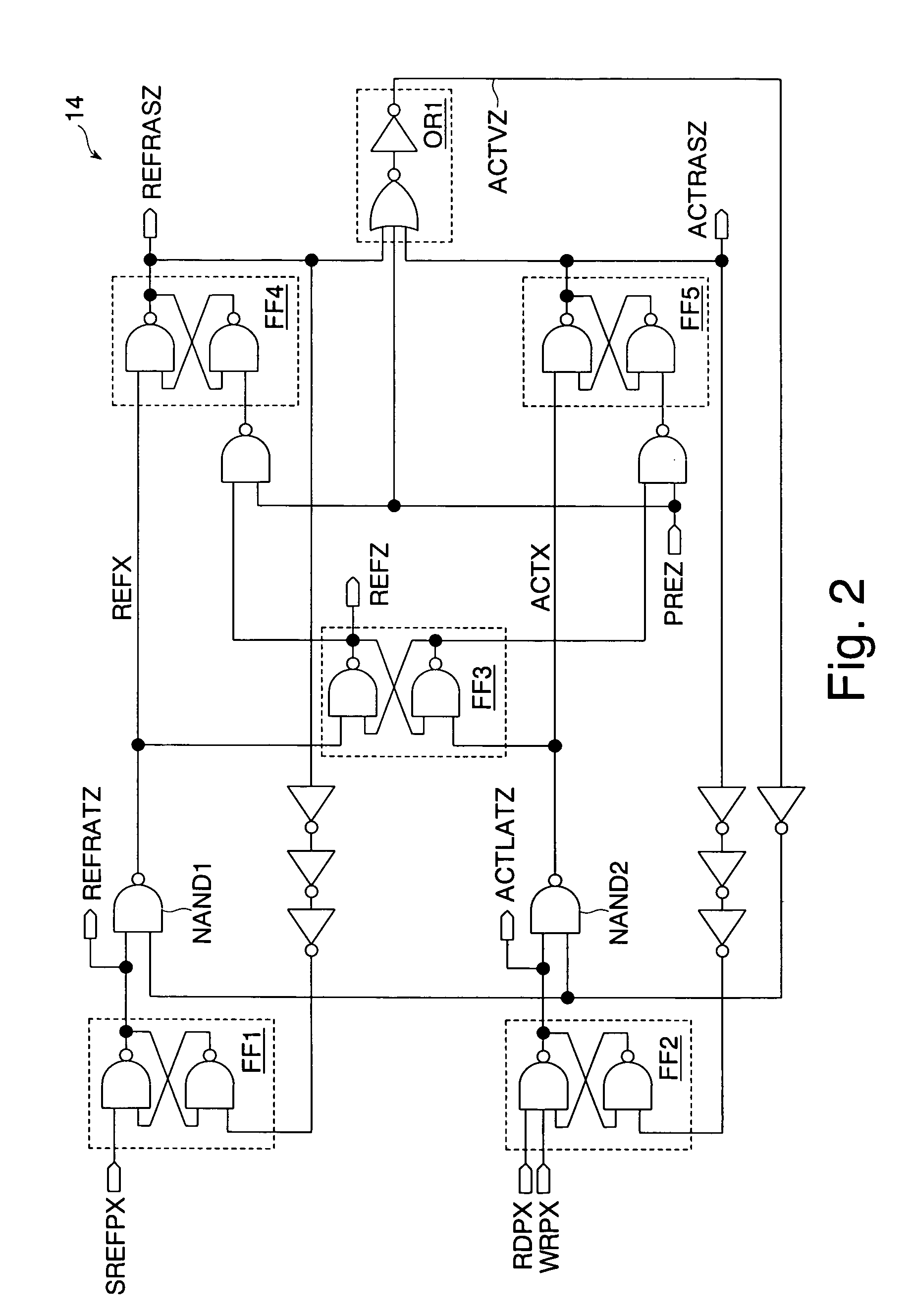
[0111] The REFRASZ counter 44, as shown in FIG. 11, resets the counter value CNT to “0” (FIG. 11(a, b, c)) in synchronism with the activation of the access timing signal ACTRASZ responding to the access request RDPX (or WRPX). In synchronism with the activation of the refresh timing signal REFRASZ responding to the refresh request SREFPX, on the other hand, the REFRASZ counter 44 performs the counting operation to increase the counter value CNT (FIG. 11 (d, e, f)). When the counter value CNT becomes “2”, the REFRASZ counter 44 changes the enable signal ENZ from the low level to the high level (FIG. 11(g)).
[0112] For th
third embodiment
[0118]FIG. 14 shows an example of the third embodiment, in which the access command (RD or WR) is supplied during the precharge operation after the refresh operation REF. The BRSVPPZ generating circuit 46 receives the access latch signal ACTLATZ activated in response to the access command, and changes the BRS setting signal BRSVPPZ from the low level to the high level in synchronism with the access latch signal ACTLATZ (FIG. 14(a)). The BRS generating circuit 28 receives the BRS setting signal BRSVPPZ at the high level, and changes the high-level voltage VBRS of the bit line resetting signal BRS from the internal supply voltage VII to the boost voltage VPP (FIG. 14(b)). As a result, the high-level voltage of the bit line resetting signal BRS is switched during the precharge operation from the internal supply voltage VII to the boost voltage VPP (FIG. 14(c)). Therefore, it is possible to shorten the precharge period after the refresh operation REF. As a result, the time period from the
PUM
 Abstract
Description
Claims
Application Information
 - R&D Engineer
- R&D Manager
- IP Professional
- Industry Leading Data Capabilities
- Powerful AI technology
- Patent DNA Extraction
Browse by: Latest US Patents, China's latest patents, Technical Efficacy Thesaurus, Application Domain, Technology Topic.
© 2024 PatSnap. All rights reserved.Legal|Privacy policy|Modern Slavery Act Transparency Statement|Sitemap