Semiconductor memory device
a memory device and semiconductor technology, applied in the direction of information storage, static storage, digital storage, etc., can solve the problem of being unable to set enough write time to write data in a memory cell
- Summary
- Abstract
- Description
- Claims
- Application Information
AI Technical Summary
Benefits of technology
Problems solved by technology
Method used
Image

Examples
first embodiment
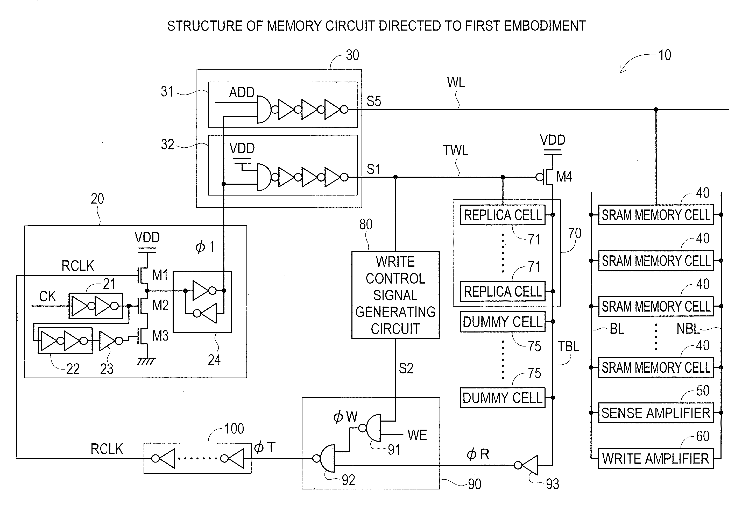
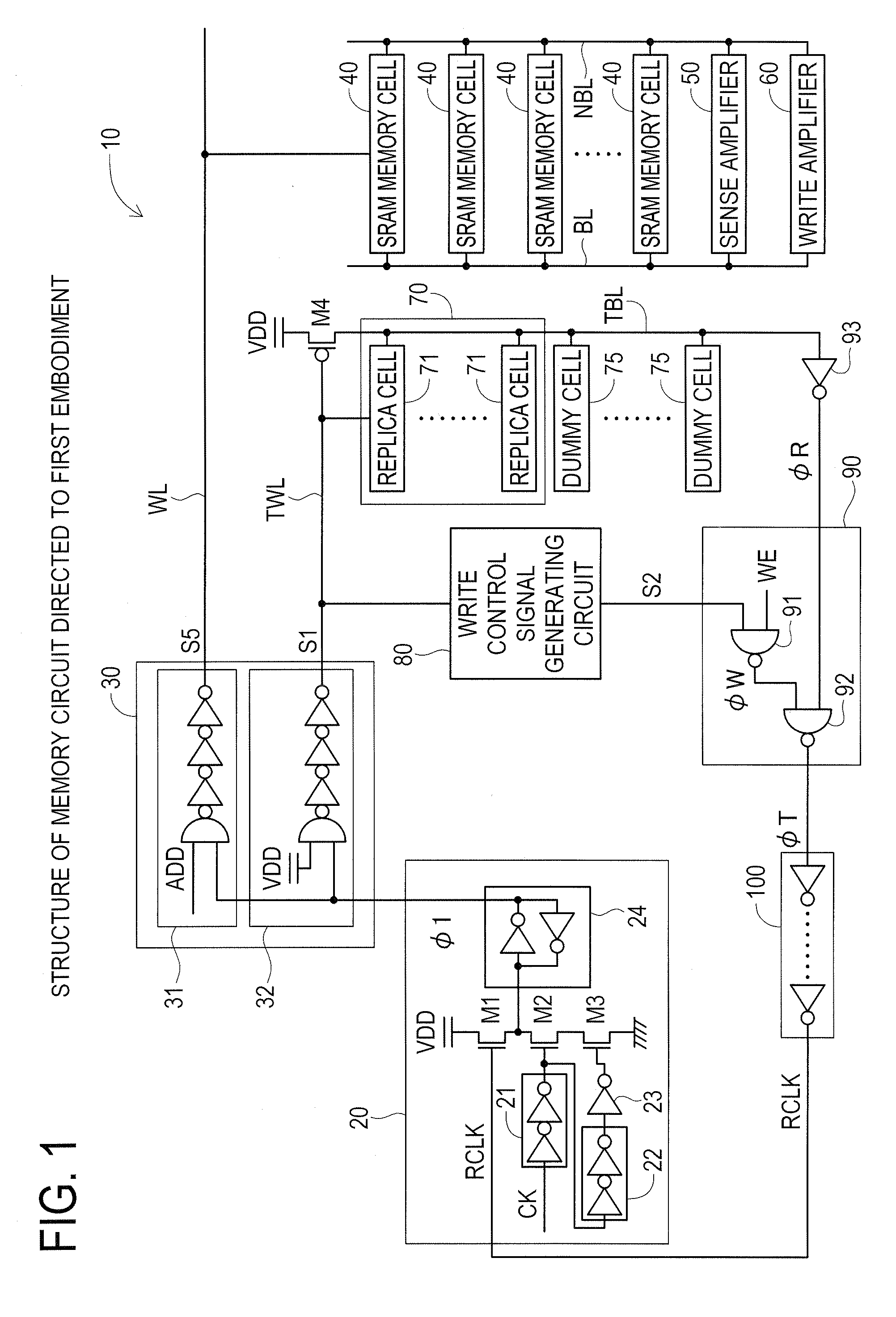
[0021]A first embodiment of the present disclosure will next be described with reference to FIG. 1 and FIG. 2. Here, the semiconductor memory device of the present disclosure will be described taking as example a memory circuit comprising SRAM. FIG. 1 is a diagram showing the structure of a memory circuit 10. The memory circuit 10 has a memory control circuit 20, a word line driver 30, SRAM memory cells 40, a sense amplifier 50, a write amplifier 60, a replica circuit 70, a write control signal generating circuit 80, a signal selection circuit 90 and a first delay adjustment circuit 100.
[0022]The memory control circuit 20 has a first delay circuit 21, a second delay circuit 22, an inverter 23, N-type transistors M1 through M3, and a latch circuit 24.
[0023]An output terminal of the first delay circuit 21 is connected to a gate of an N-type transistor M2 and an input terminal of a second delay circuit 22. An output terminal of the second delay circuit 22 is connected to an input of the i
second embodiment
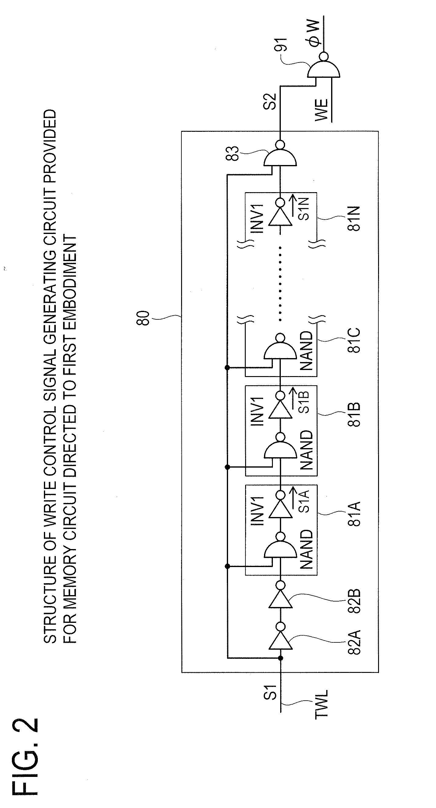
[0073]A second embodiment of the present disclosure will now be described with reference to FIG. 5. A memory circuit of the present embodiment has a write control signal generating circuit 80A shown in FIG. 5, in place of the write control signal generating circuit 80 in the first embodiment. The write control signal generating circuit 80A has second signal generating units 84A through 84N and inverters 85A through 85M, and P-type transistors 86A through 86M. Here, the second signal generating units 84C through 84M, inverters 85C through 85M and P-type transistors 86C through 86M are not shown in the drawing.
[0074]The second signal generating units 84A through 84N respectively comprise an inverter INV4 and an N-type transistor M5. An input of each inverter INV4 is connected to an input terminal of each second signal generating unit 84A through 84N. An output of each inverter INV4 is connected to a source of each N-type transistor M5. A power source voltage VDD is applied to a gate of e
PUM
 Abstract
Description
Claims
Application Information
 - R&D Engineer
- R&D Manager
- IP Professional
- Industry Leading Data Capabilities
- Powerful AI technology
- Patent DNA Extraction
Browse by: Latest US Patents, China's latest patents, Technical Efficacy Thesaurus, Application Domain, Technology Topic.
© 2024 PatSnap. All rights reserved.Legal|Privacy policy|Modern Slavery Act Transparency Statement|Sitemap