Stack of semiconductor chips

a technology of semiconductor chips and stacks, which is applied in the direction of semiconductor devices, semiconductor/solid-state device details, electrical equipment, etc., can solve the problems of high assembly cost, high assembly cost, and inability to meet the requirements of reliability, so as to improve the adhesion between chips, increase the surface area accessible, and improve the effect of adhesion

Inactive Publication Date: 2007-08-02
POLARIS INNOVATIONS
View PDF6 Cites 43 Cited by
  • Summary
  • Abstract
  • Description
  • Claims
  • Application Information

AI Technical Summary

Benefits of technology

This patent describes different ways to make a type of component called a "mold cap," which helps prevent moisture ingress during manufacturing processes. By attaching a flat surface onto the top of the component, water vapor cannot enter through cracks in the component itself. This prevents damage to the underlying circuitry and improves overall performance. Overall, these technical features help create reliable packages.

Problems solved by technology

The technical problem addressed in this patent is how to efficiently package multiple chips together without damaging them during the manufacturing process while maintaining reliable connection between the chips and the substrates.

Method used


Image

  • Stack of semiconductor chips
  • Stack of semiconductor chips
  • Stack of semiconductor chips

Examples


Embodiment Construction

[0030] The making and using of the presently preferred embodiments are discussed in detail below. It should be appreciated, however, that the present invention provides many applicable inventive concepts that can be embodied in a wide variety of specific contexts. The specific embodiments discussed are merely illustrative of specific ways to make and use the invention, and do not limit the scope of the invention.

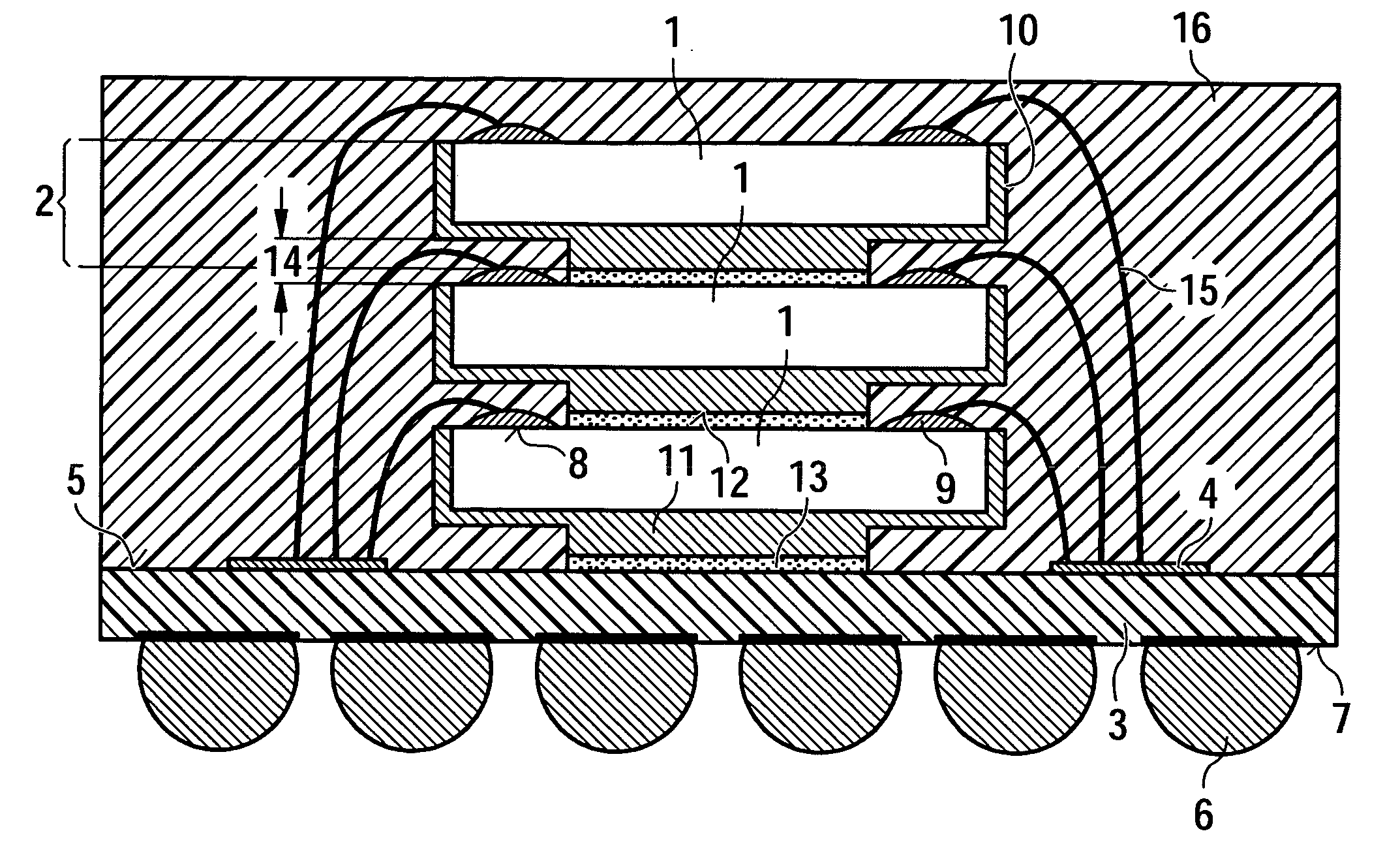
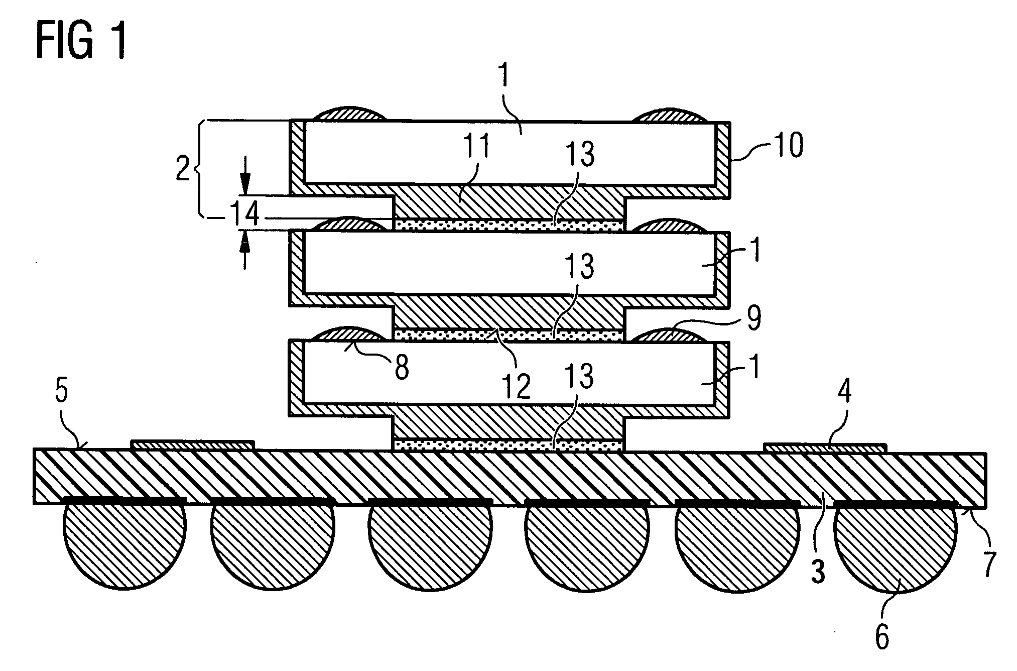
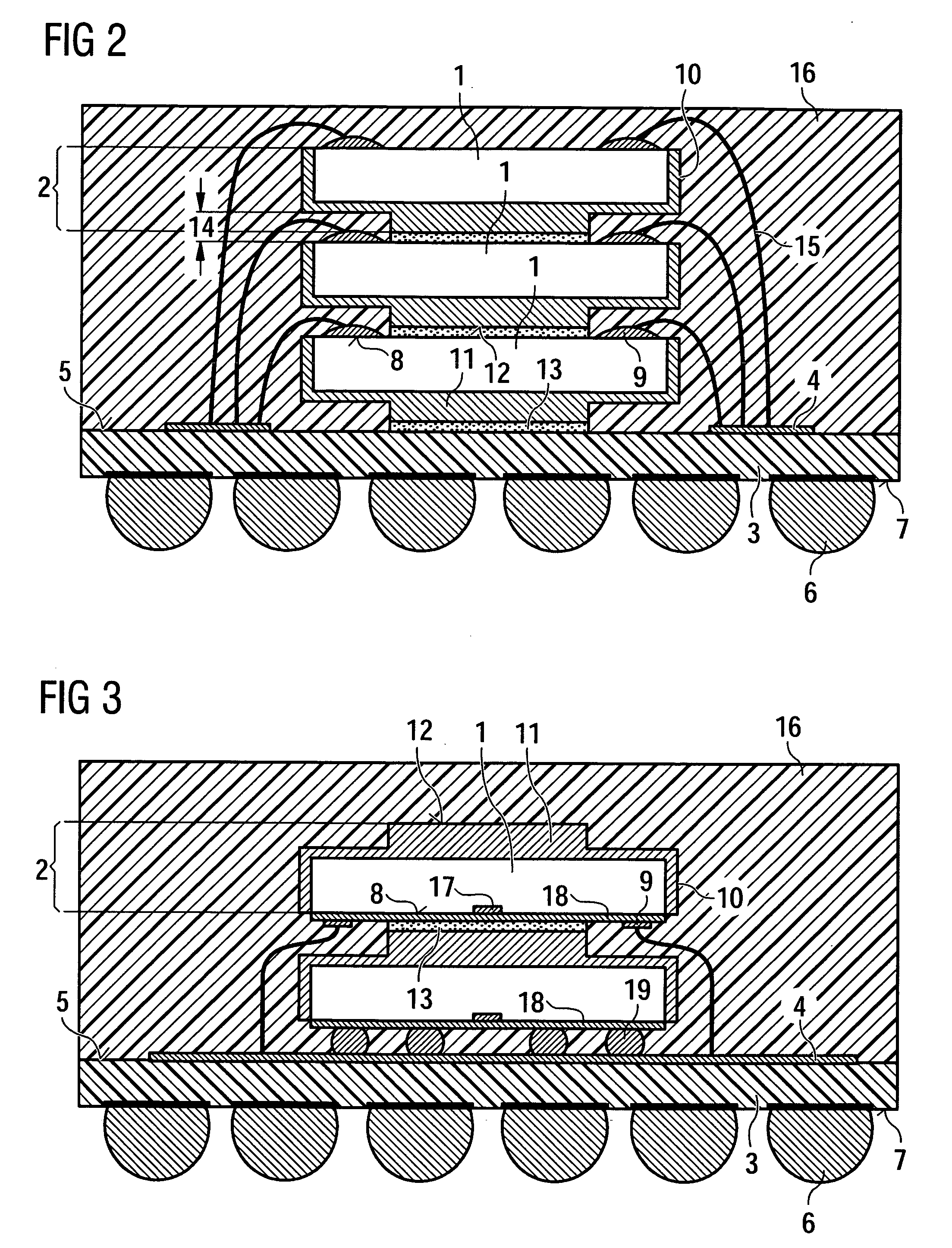
[0031]FIG. 1 shows three individual embedded semiconductor chips 1 (individual components 2) in a face-up arrangement on a carrier substrate 3. Conductor structures 4 of the upper surface 5 of the substrate 3 are electrical interconnected (not shown) with electrical contacts 6 located on the lower surface 7 of the substrate 3. In the preferred embodiments, these contacts 6 are fine pitch ball grid arrays (FBGA), by means of which the stack arrangement can be integrated into a circuit, e.g., by soldering the contacts 6 to a circuit board (not shown).

[0032] All individual chips


PUM


Abstract

A stack of semiconductor chips includes a substrate or an interposer board comprising conductor structures for electrical connection of the stack and a first chip. The first chip includes an active side with peripherally arranged bonding pads and is mounted face-up on the substrate or the interposer board. The stack beyond includes at least a further chip with peripherally arranged bonding pads on its active side. The back side and at least two chip edges of the further chip are embedded by a mold cap providing a protuberance on the back side of the chip. The protuberance forms a planar surface extending substantially parallel and with a distance to the back side of the chip. The further chip is attached face-up to the active side of the first chip by an adhesive applied between the protuberance and the first chip so that the protuberance is inserted between both chips to provide a gap there. The protuberance has at least one linear dimension that is smaller than a linear dimension of the subjacent chip.

Description


Claims


Application Information

Patent Timeline
Owner POLARIS INNOVATIONS
Why Eureka
Try Eureka