Organic semiconductor device and method of fabricating the same

Inactive Publication Date: 2008-02-07
IND TECH RES INST
View PDF3 Cites 0 Cited by
  • Summary
  • Abstract
  • Description
  • Claims
  • Application Information

AI Technical Summary

Benefits of technology

[0008]The present invention is directed to an organic semiconductor device and a meth

Problems solved by technology

Though OTFT has the above described advantages, some drawbacks such as slow carrier mobility and high driving voltage are needed to be solved.
Thus, the carrier mobility is slowed down, and electrical characteristics of devices are affected, thereby restricting the development and applications of the OTFT.
However,

Method used


Image

  • Organic semiconductor device and method of fabricating the same
  • Organic semiconductor device and method of fabricating the same
  • Organic semiconductor device and method of fabricating the same

Examples


Embodiment Construction

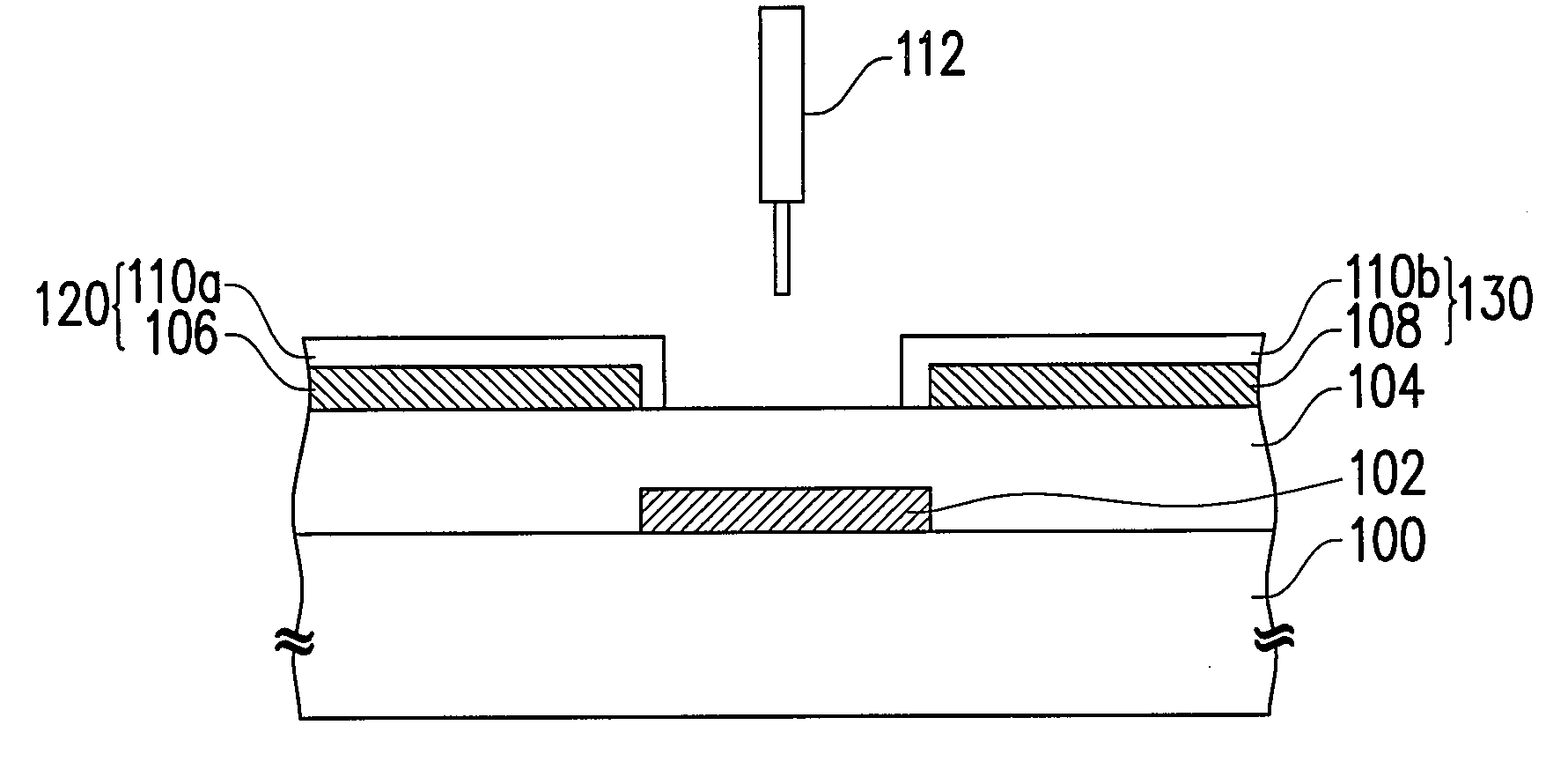
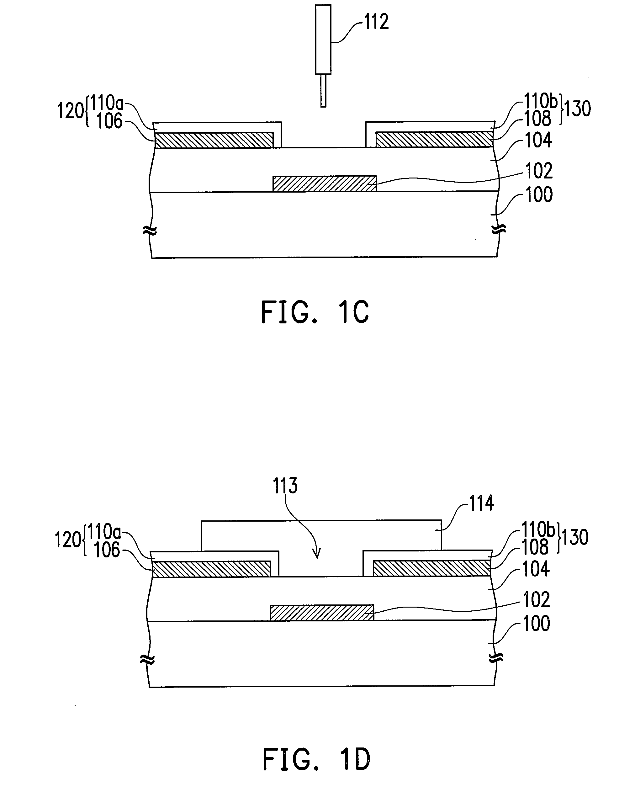
[0019]In the present invention, an organic conductive layer is added between the metal electrode and the organic semiconductor active layer, and it has a work function matching with the semiconductor material. In addition, the present invention can also help the arrangement of the organic semiconductor grains and make the grains of the organic semiconductor active layer on the metal electrode become larger, so as to improve the carrier mobility of the device. The present invention can be applied to the organic semiconductor devices, and is described as follows.

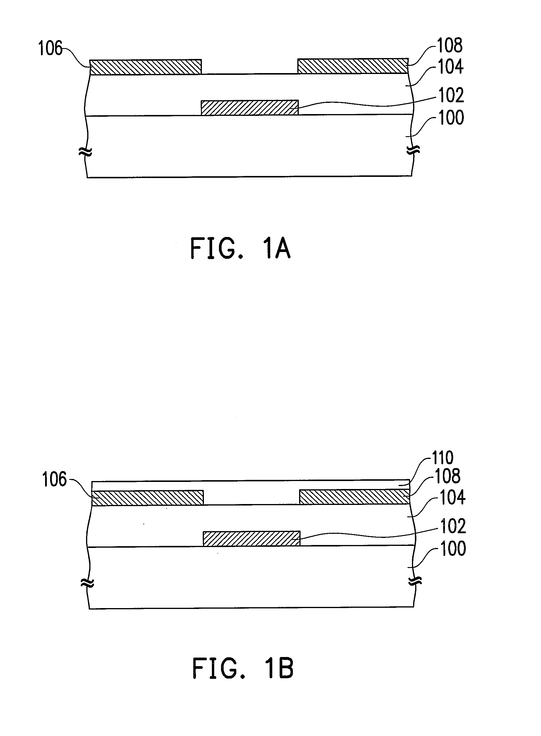
[0020]FIGS. 1A to 1D are cross-sectional views illustrating a method for fabricating an organic semiconductor device according to an embodiment of the present invention.

[0021]Please refer to FIG. 1A, a gate conductive layer 102 is formed on a substrate 100. The substrate 100 can be a flexible substrate or a rigid substrate, wherein the material of the flexible substrate is plastic, for example, and the material of the rigid subst


PUM


Abstract

An organic semiconductor device is provided. A conductive gate layer and a gate dielectric layer are formed on a substrate. Patterned metal layers are formed on the gate dielectric layer beside the conductive gate layer. An electrode modified layer is formed on a top surface and sidewall of each of the patterned metal layer. The patterned metal layers and the electrode modified layers formed thereon serve a source and a drain. An organic semiconductor layer is formed on the source and the drain.

Description


Claims


Application Information

Patent Timeline
Owner IND TECH RES INST
Why Eureka
Try Eureka