Liquid crystal display device and fabrication method thereof

Active Publication Date: 2008-07-24
LG DISPLAY CO LTD
View PDF5 Cites 10 Cited by
  • Summary
  • Abstract
  • Description
  • Claims
  • Application Information

AI Technical Summary

Benefits of technology

[0031]Another object of the embodiments of the invention is to provide an LCD and its fabrication method capable of implementing high picture quality without generating a wavy noise, and capable of implementing high luminance by

Problems solved by technology

In particular, because the masks designed for forming the pattern are quite expensive, as the number of masks used in the processes increases, the f

Method used


Image

  • Liquid crystal display device and fabrication method thereof
  • Liquid crystal display device and fabrication method thereof
  • Liquid crystal display device and fabrication method thereof

Examples


first embodiment

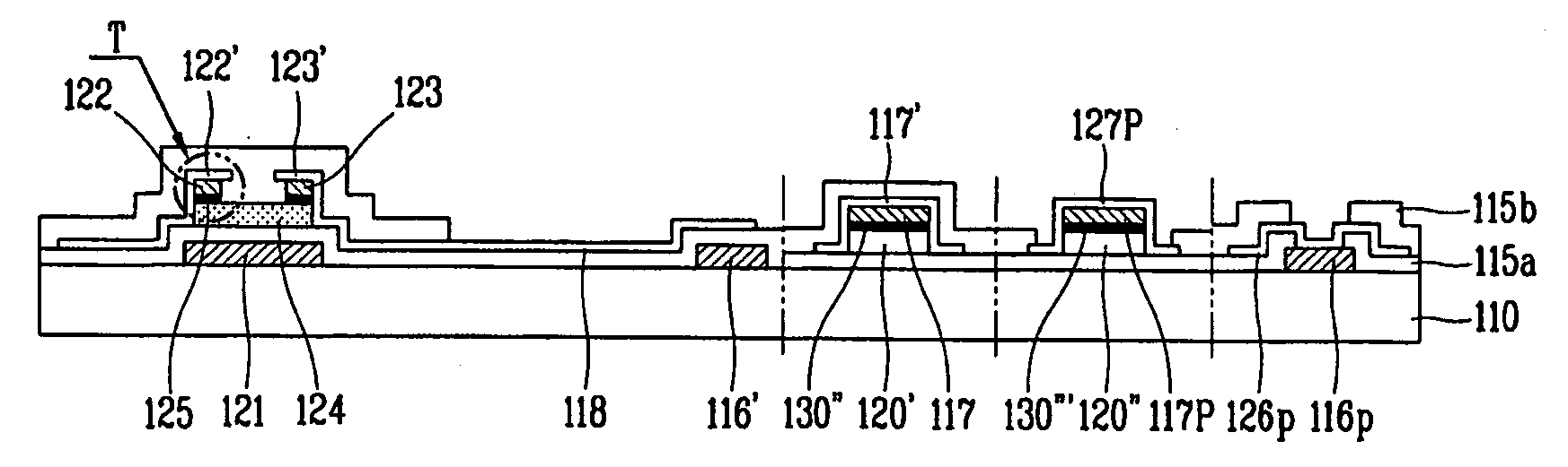
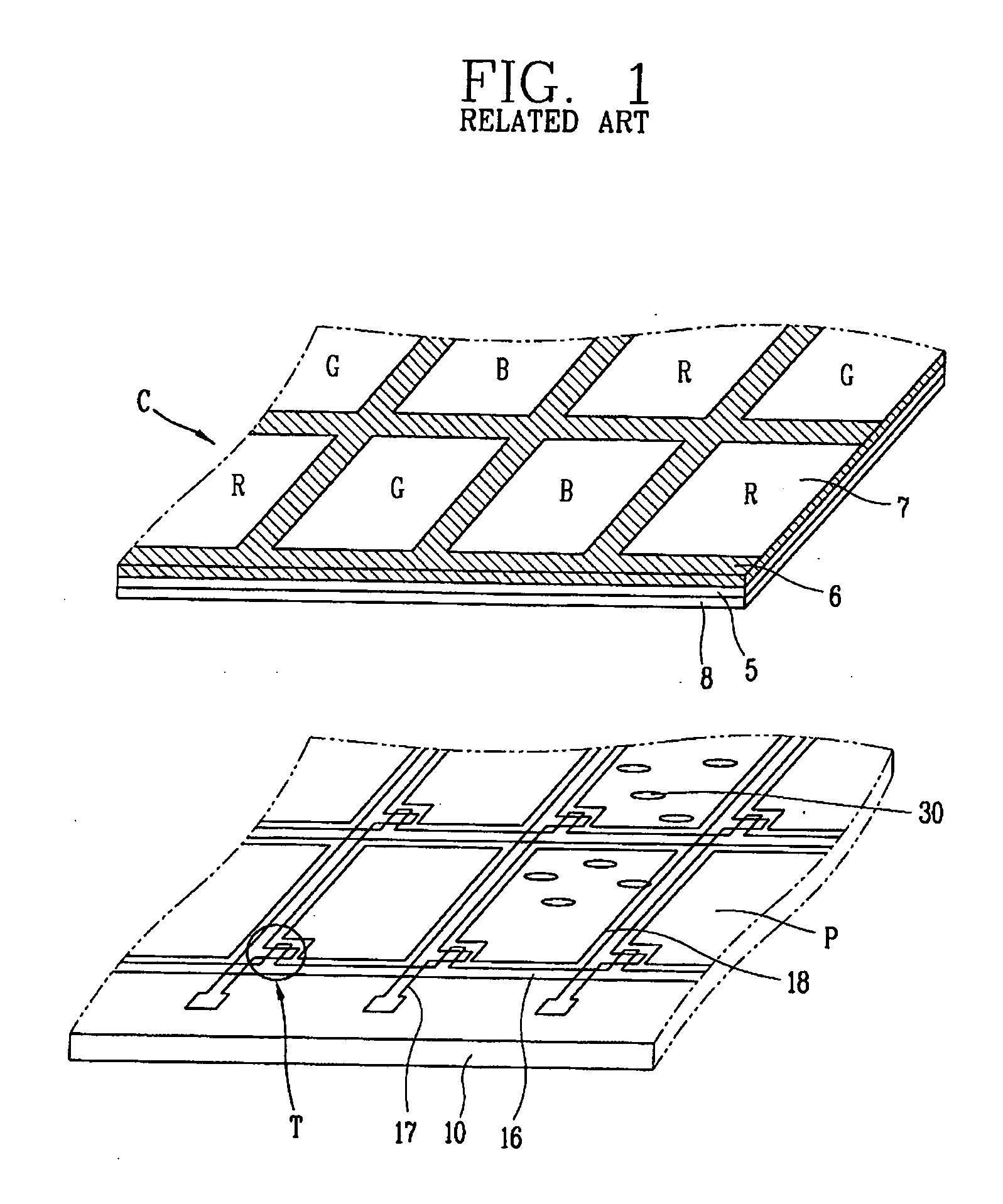
[0053]FIG. 3 is a plan view showing a portion of an array substrate of an LCD according to the present invention, in which a single pixel including a gate pad part and a data pad part are shown for the sake of explanation.

[0054]FIG. 4 is a view illustrating an enlarged portion ‘A’ of the array substrate in FIG. 3.

[0055]Actually, the N number of gate lines and the M number of data lines are formed to cross each other to define the M×N number of pixels. To simplify the explanation, only a single pixel is shown.

[0056]As shown in FIGS. 3 and 4, on an array substrate 110 according to a first embodiment of the present invention, gate lines 116 and the data lines are formed to be arranged vertically and horizontally to define the pixel region. A thin film transistor (TFT), a switching element, is formed at a crossing of the gate line 116 and the data line 117. A pixel electrode 118 is formed within the pixel region, is connected with the TFT to drive liquid crystal (not shown) together with a

second embodiment

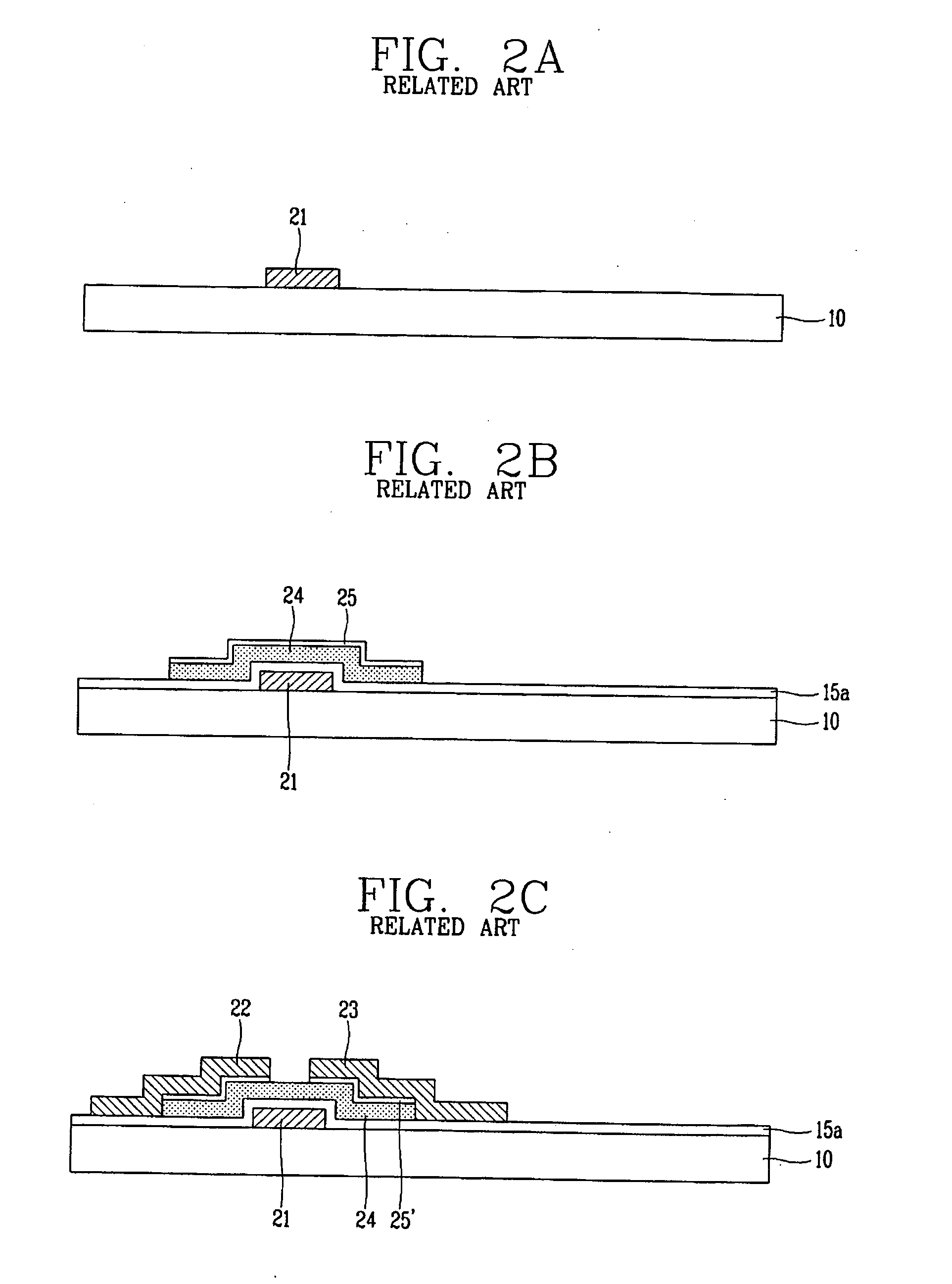
[0114]In order to improve this structure, the photosensitive film pattern is collapsed through a baking process after the first wet etching to cover the upper conductive film pattern, and then, the second wet etching is performed to thus prevent the occurrence of the above-mentioned undercut phenomenon and form a forward taper shape. This will now be described in detail through the present invention.

[0115]FIGS. 9A to 9E are cross-sectional views sequentially showing an etching process in the two-metal stacked structure according to a second embodiment of the present invention.

[0116]As shown in FIG. 9A, a first conductive film 260 and a second conductive film 265 are stacked on an array substrate 210, and then, a first photosensitive film pattern 275 made of a photosensitive material such as photoresist is formed thereon.

[0117]Thereafter, as shown in FIG. 9B, the lower second conductive film is selectively removed by using the first photosensitive film pattern 275 as a mask (a first wet


PUM


Abstract

A liquid crystal display (LCD) device includes: a first substrate divided into a pixel part and first and second pad parts; a gate electrode and a gate line formed at the pixel part of the first substrate; an active pattern as an island formed over the gate electrode with a first insulation film interposed therebetween, and having a width smaller than the gate electrode; an ohmic-contact layer formed on source and drain regions of the active pattern on the first substrate; source and drain electrodes formed as islands over the gate electrode of the first substrate and electrically connected with the source and drain regions of the active pattern via the ohmic-contact layer; a data line formed on the pixel part of the first substrate and crossing the gate line to define a pixel region; a pixel electrode formed at the pixel region and electrically connected with the drain electrode; a second insulation film formed on the first substrate; and a second substrate attached to the first substrate in a facing manner.

Description


Claims


Application Information

Patent Timeline
Owner LG DISPLAY CO LTD
Why Eureka
Try Eureka