Light emitting diode structure

a technology of light-emitting diodes and diodes, which is applied in the direction of basic electric elements, electrical equipment, and semiconductor devices, can solve the problems of short operation life, high power consumption, and low efficiency of light-emitting diodes, and achieve the effect of improving the reliability of light-emitting diodes

Inactive Publication Date: 2008-10-23
EVERLIGHT ELECTRONICS
View PDF3 Cites 13 Cited by
  • Summary
  • Abstract
  • Description
  • Claims
  • Application Information

AI Technical Summary

Benefits of technology

This invention relates to improving the performance of LEDs that use different materials for their components. By placing an insulating material called BARC (Bathylene-based Acrylic Resin) on top of each component's interface with other parts during manufacturing process, it prevents certain metals from being absorbed inside them when they are used together due to differences in crystal structures caused by temperature changes. Additionally, this design helps improve the efficiency at which heat generated within these devices can escape through its substrate.

Problems solved by technology

This patented technical problem addressed by this patents relates to improving the performance and lifetimes of LED lights used for various purposes like indoor decoration without harmful effects caused from their use at very hot temperatures or with strong electrical current.

Method used


Image

  • Light emitting diode structure
  • Light emitting diode structure

Examples


Embodiment Construction

[0014]Reference will now be made in detail to the present preferred embodiments of the invention, examples of which are illustrated in the accompanying drawings. Wherever possible, the same reference numbers are used in the drawings and the description to refer to the same or like parts.

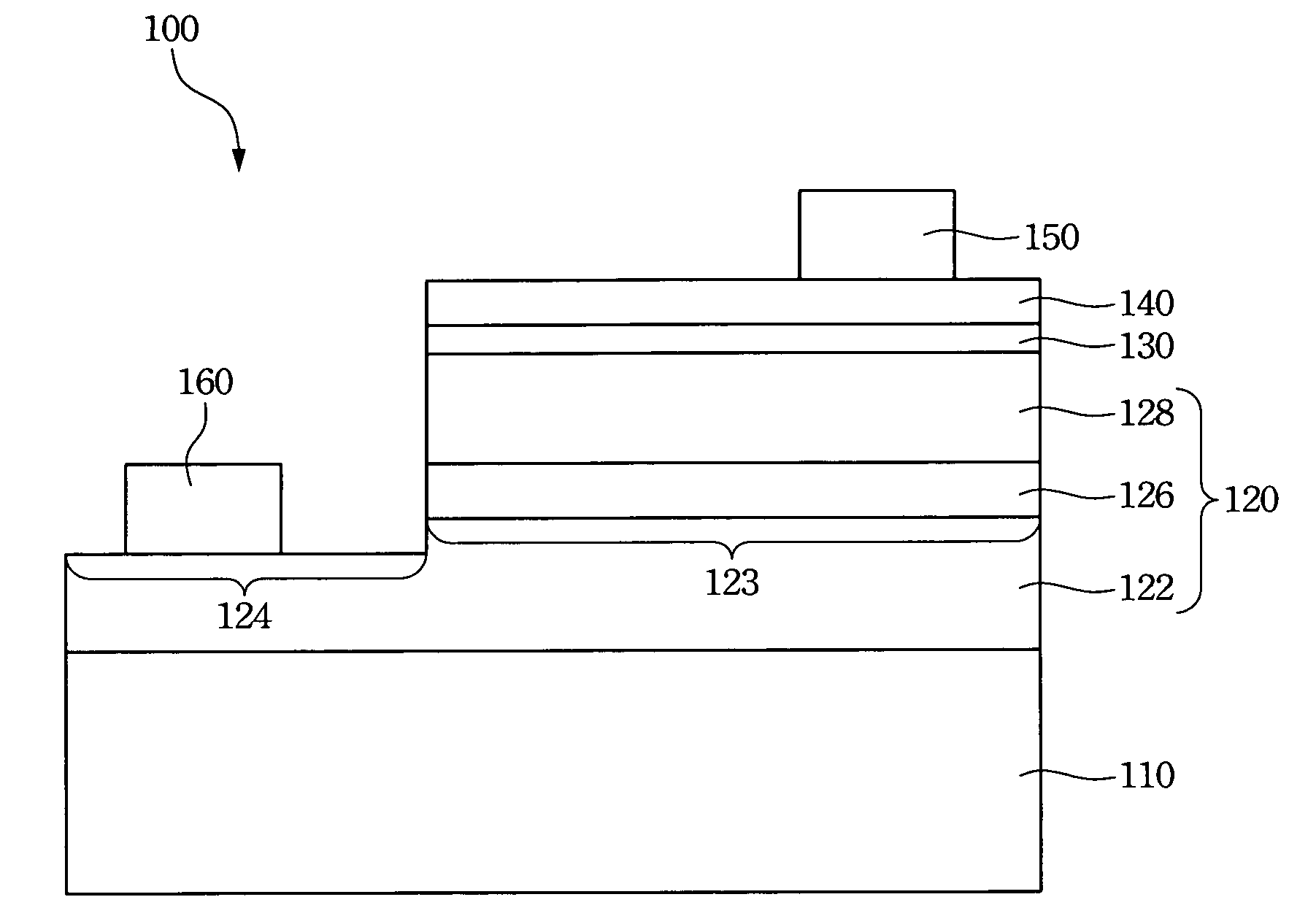
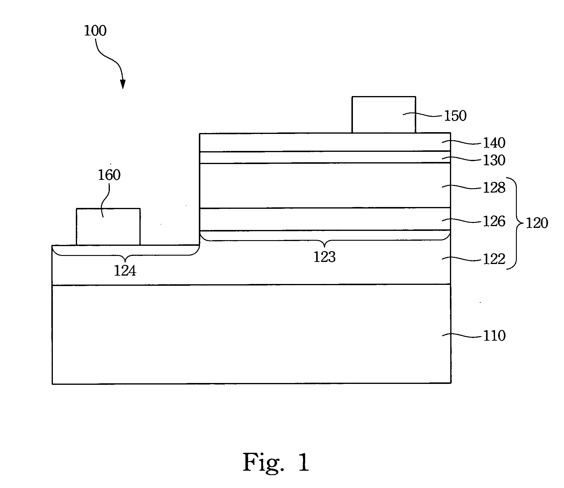
[0015]Refer to FIG. 1. FIG. 1 illustrates a cross-section view diagram of an embodiment of the light-emitting diode structure of the invention. The light-emitting diode structure 100 includes a substrate 110, a semiconductor laminated layers 120 formed on the substrate 110, a barrier layer 130 formed on the semiconductor laminated layers 120, and a contact layer 140 formed on the barrier layer 130. The contact layer 140 may be a metal layer. The barrier layer 130 of the light-emitting diode structure 100 may prevent the metal atoms of the contact layer 140 diffusing into the semiconductor laminated layers 120, and also reduce the reaction or the phase transformation between the contact layer 140 and the


PUM


Abstract

The light emitting diode structure includes a substrate, a first electricity semiconductor layer formed on the substrate, a light-emitting layer formed on the first electricity semiconductor layer, a second electricity semiconductor layer formed on the light-emitting layer, a barrier layer formed on the second electricity semiconductor layer, and a contact layer formed on the barrier layer.

Description


Claims


Application Information

Patent Timeline
Owner EVERLIGHT ELECTRONICS
Why Eureka
Try Eureka