Semiconductor device and method of manufacturing the same
- Summary
- Abstract
- Description
- Claims
- Application Information
AI Technical Summary
Benefits of technology
Problems solved by technology
Method used
Image

Examples
first embodiment
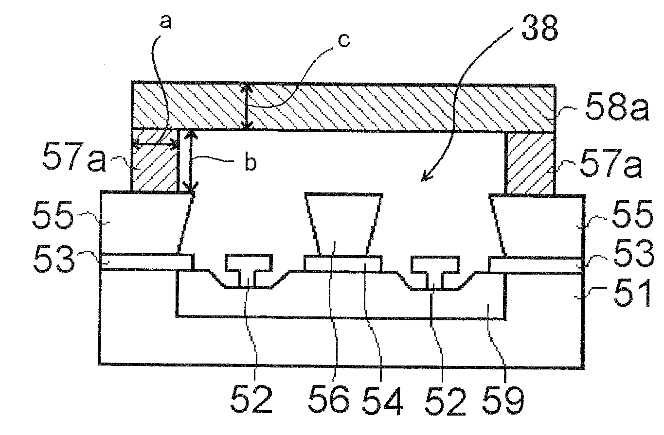
[0028]A semiconductor device of the first embodiment will be explained referring to a sectional view shown in FIG. 1. FIG. 1 shows an exemplary case where a semiconductor device is placed on a lead frame.
[0029]As shown in FIG. 1, a semiconductor device 30 has a semiconductor element 32, a frame component 36 provided over the semiconductor element 32 while forming a cavity 38 therein, and a molding resin layer 42 covering around the frame component 36. Electrode pads of the semiconductor element 32 are electrically connected via wires 40 to a lead frame 31.
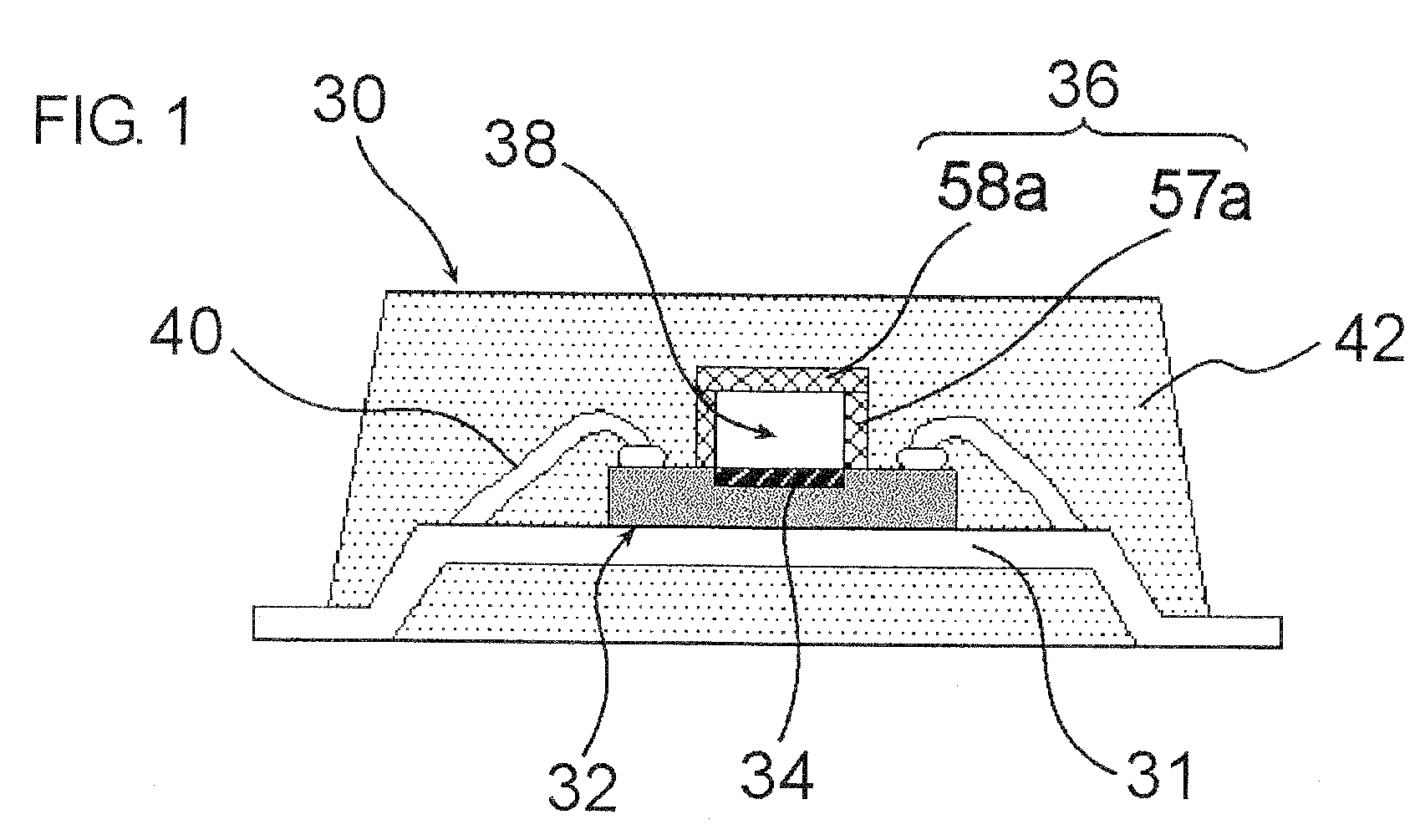
[0030]The frame component 36 has a hollow structure composed of a first resin film 57a provided as being risen up around an active region 34 of the semiconductor element 32, and a second resin film 58a tightly closing the space surrounded by the first resin film 57a. As shown in FIG. 3B, given as a partially enlarged view of the frame component 36, the thickness “a” of the first resin film 57a is approximately 5 to 50 μm, and the heig
second embodiment
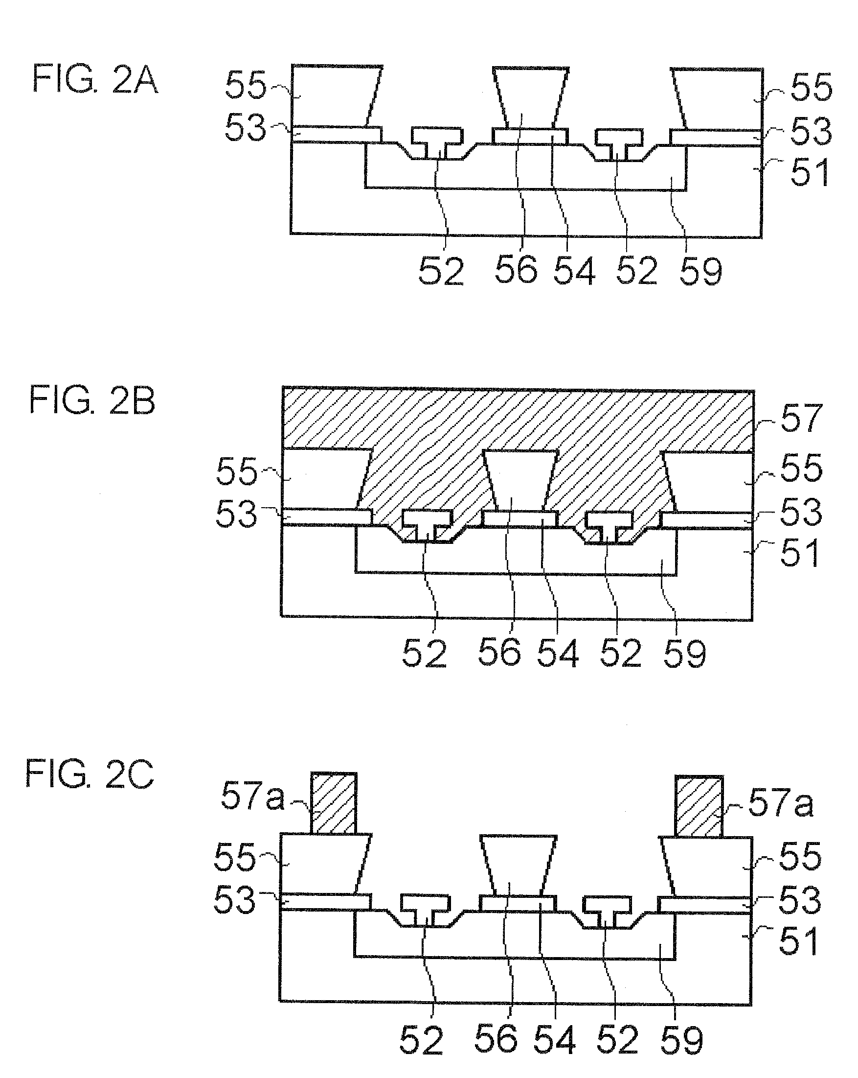
[0067]FIG. 5 shows a semiconductor device of a In this embodiment, the first resin film 57a is left unremoved not only around the gate, but also around the pads. This configuration raises an advantage in that the cavity may be formed in a stable manner, when the photosensitive sheet-like second resin film 58 is bonded.
[0068]FIG. 6 shows a semiconductor device of a third embodiment. In this embodiment, contact area between the first resin film 57a and the second resin film 58a is increased as compared with that in the second embodiment. By virtue of this configuration, adhesiveness between the resins may be made stronger, and thereby yield ratio of the semiconductor device may be improved.
[0069]FIG. 7 shows a semiconductor device of a fourth embodiment. Although this embodiment has a structure different in arrangement of the gates, sources and drain from those in the first to third embodiments, the active region 34 may be covered with the frame component 36 having the cavity 38 therein
PUM
 Abstract
Description
Claims
Application Information
 - R&D Engineer
- R&D Manager
- IP Professional
- Industry Leading Data Capabilities
- Powerful AI technology
- Patent DNA Extraction
Browse by: Latest US Patents, China's latest patents, Technical Efficacy Thesaurus, Application Domain, Technology Topic.
© 2024 PatSnap. All rights reserved.Legal|Privacy policy|Modern Slavery Act Transparency Statement|Sitemap