Compound semiconductor substrate
- Summary
- Abstract
- Description
- Claims
- Application Information
AI Technical Summary
Benefits of technology
Problems solved by technology
Method used
Image

Examples
first embodiment
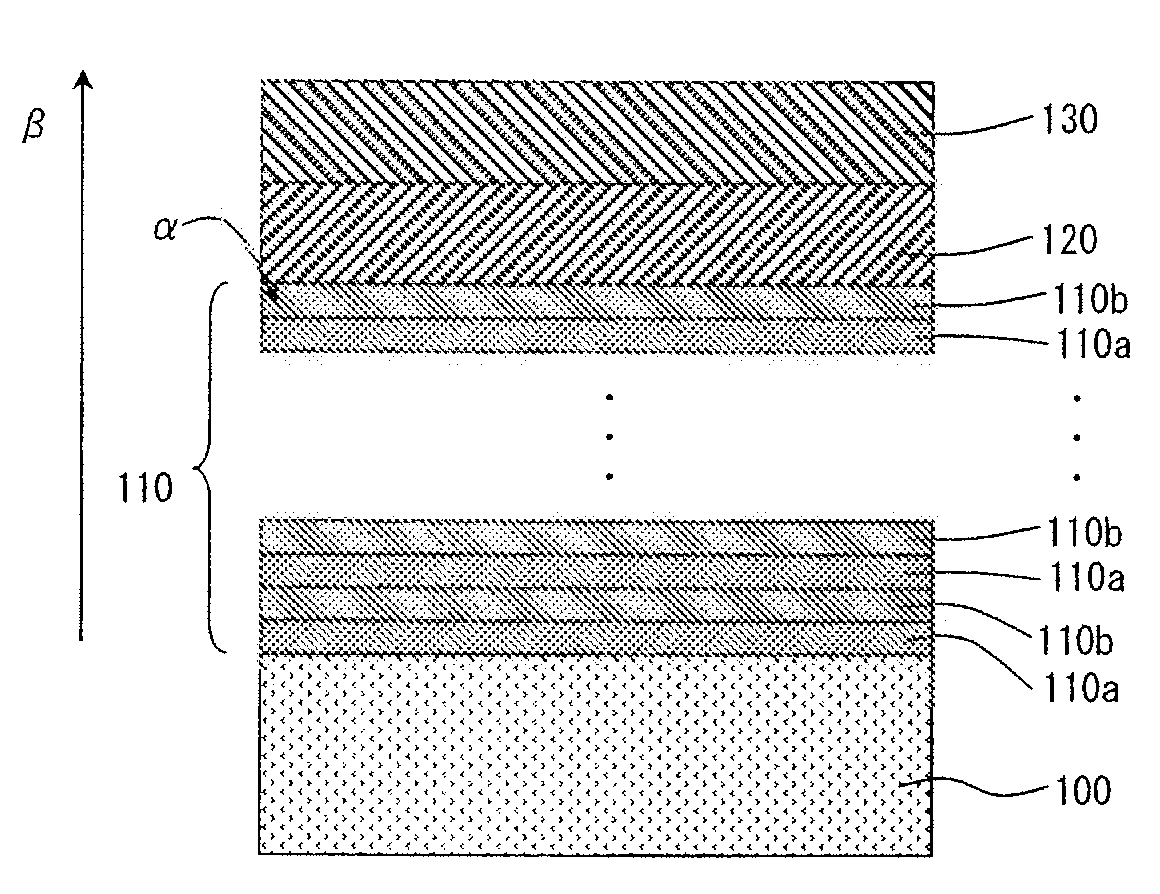
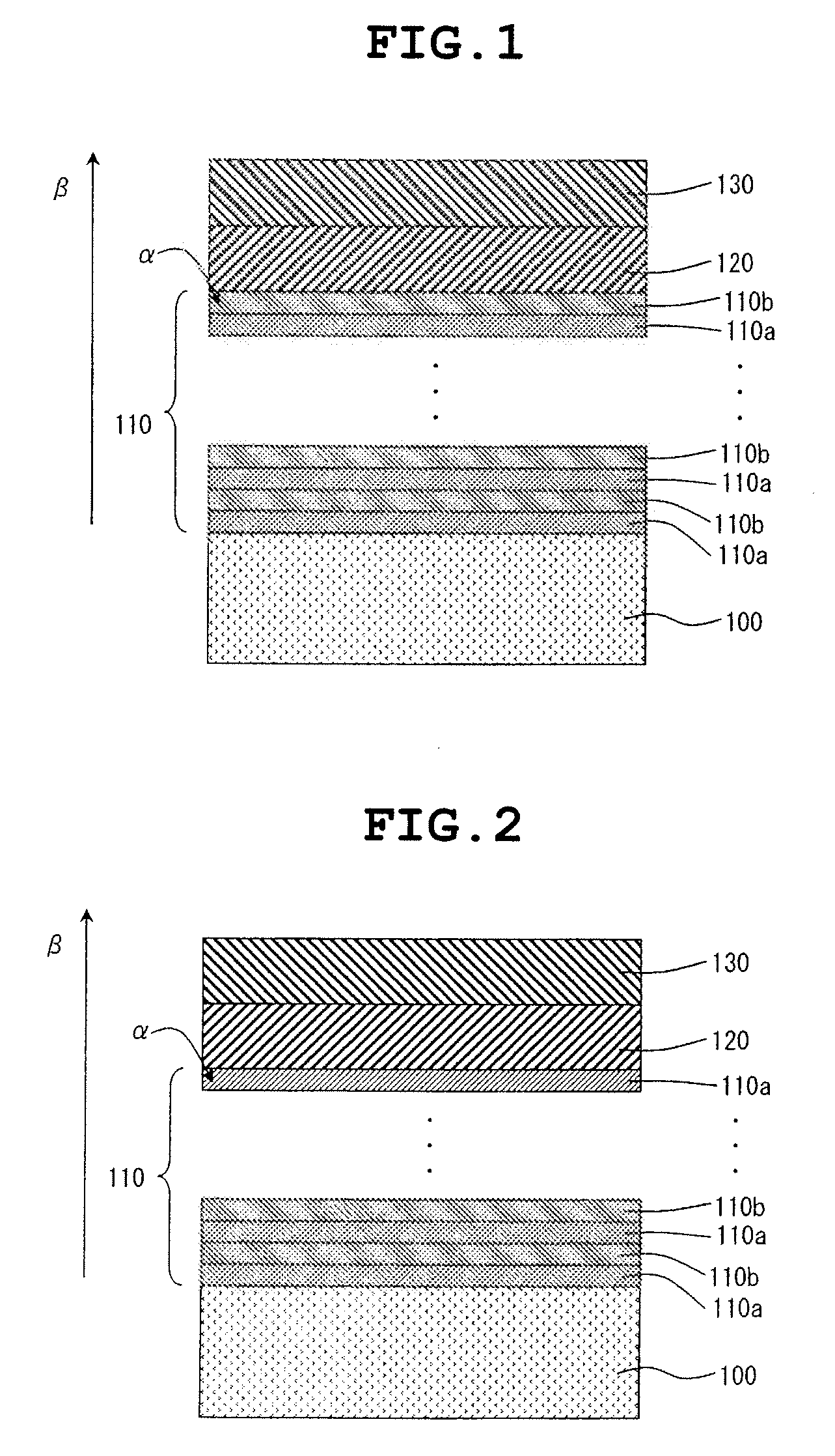
[0047]FIGS. 1 and 2 are each a sectional view illustrating a compound semiconductor substrate according to a first embodiment of the invention.
[0048]As illustrated in FIGS. 1 and 2, the compound semiconductor substrate according to the present embodiment has a structure which are successively formed a first intermediate layer 110, a second intermediate layer 120 and a compound semiconductor single crystal layer 130 on a Si single crystal substrate 100.
[0049]The Si single crystal substrate 100 is a Si single crystal substrate having a surface having a crystal plane orientation of a {111} plane. The plane orientation {111} may be a fine inclination (about more than ten degrees) of any normal crystal plane orientation {111}, or any one of crystal plane orientations having higher-order Miller indices, such as {211}. When the crystal plane orientation of the surface of the Si single crystal substrate 100 is made into {111} in this way, the generation of anti-phase boundary defects is decrea
second embodiment
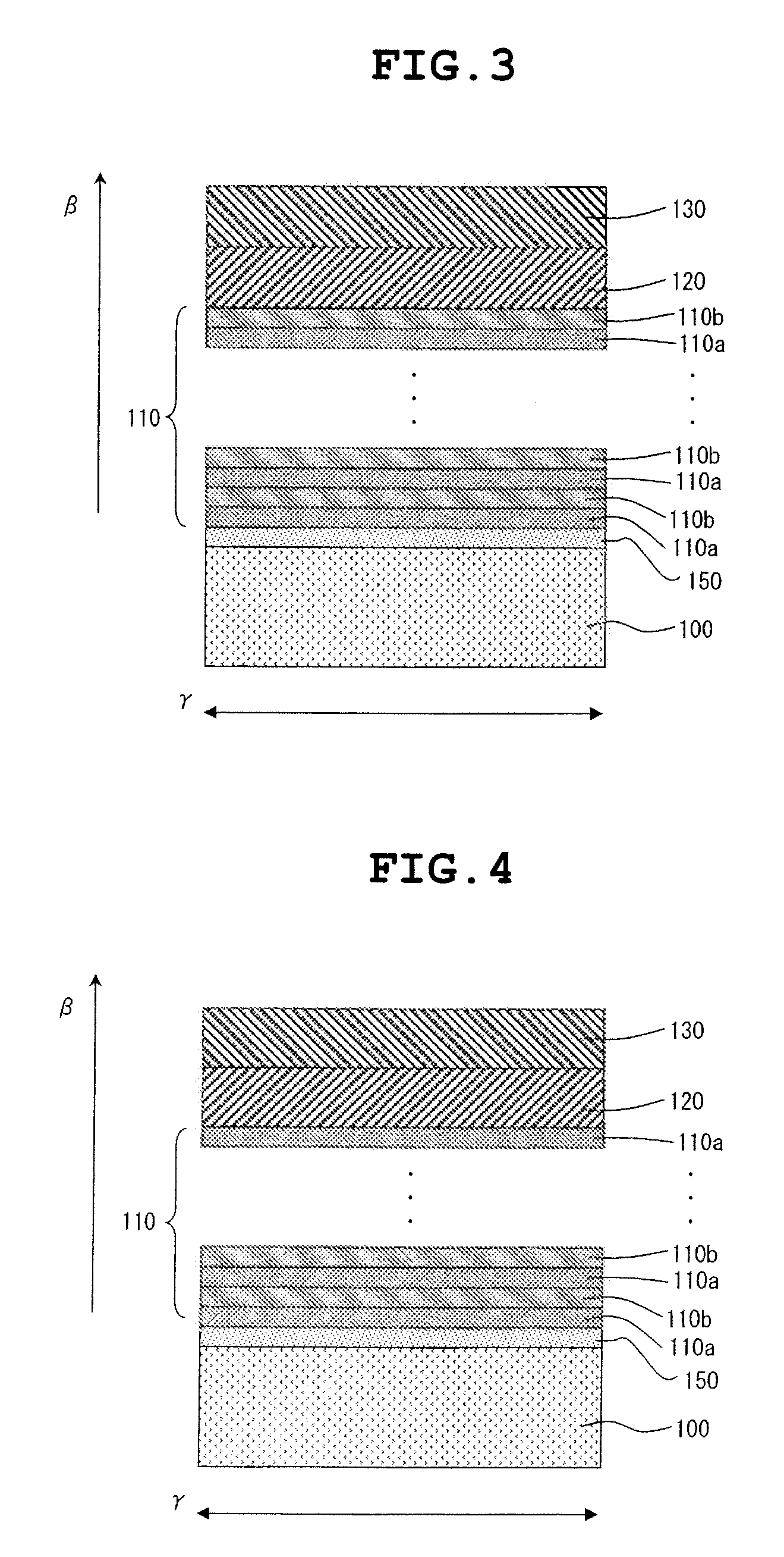
[0083]FIGS. 3 and 4 are each a sectional view illustrating a compound semiconductor substrate according to a second embodiment of the invention.
[0084]The compound semiconductor substrate according to the embodiment is different from the first embodiment in that a 3C—SiC single crystal layer 150 is formed between the first intermediate layer 110 and the Si single crystal substrate 100. Since the others are the same as in the first embodiment, description thereof is omitted.
[0085]Specifically, as illustrated in FIGS. 3 and 4, in the compound semiconductor substrate according to the embodiment, the 3C—SiC single crystal layer 150 is formed on the Si single crystal substrate, which has a crystal plane orientation of a {111} plane, and further the same first intermediate layer 110 as described in the first embodiment is formed on the 3C—SiC single crystal layer 150.
[0086]The film thickness of the 3C—SiC single crystal layer 150 preferably ranges from 10 to 800 nm. If the film thickness is l
third embodiment
[0089]FIGS. 5 and 6 are each a sectional view illustrating a compound semiconductor substrate according to a third embodiment of the invention.
[0090]As illustrated in FIGS. 5 and 6, the compound semiconductor substrate according to the present embodiment has a structure which are successively formed a first intermediate layer 210, a second intermediate layer 220 and a compound semiconductor single crystal layer 230 on a Si single crystal substrate 200.
[0091]The Si single crystal substrate 200 may be identical to the Si single crystal substrate 100 described about the first embodiment.
[0092]As illustrated in FIG. 5 or 6, in the first intermediate layer 210, a 3C—SiC single crystal layer 210a and a metal compound layer 210b are laminated, over the Si single crystal substrate 200, in this order repeatedly so as to alternate the resultant 3C—SiC single crystal layers 210a with the resultant metal compound layers 210b and render the topmost layer α of the laminate one of the 3C—SiC single c
PUM
 Abstract
Description
Claims
Application Information
 - R&D Engineer
- R&D Manager
- IP Professional
- Industry Leading Data Capabilities
- Powerful AI technology
- Patent DNA Extraction
Browse by: Latest US Patents, China's latest patents, Technical Efficacy Thesaurus, Application Domain, Technology Topic.
© 2024 PatSnap. All rights reserved.Legal|Privacy policy|Modern Slavery Act Transparency Statement|Sitemap