Electronic Device Including a Contact Structure Contacting a Layer

Active Publication Date: 2020-05-07
SEMICON COMPONENTS IND LLC
View PDF0 Cites 0 Cited by
  • Summary
  • Abstract
  • Description
  • Claims
  • Application Information

AI Technical Summary

Problems solved by technology

On-state resistance between a source and drain within a power transistor can result in power loss within the transistor.
Even w

Method used


Image

  • Electronic Device Including a Contact Structure Contacting a Layer
  • Electronic Device Including a Contact Structure Contacting a Layer
  • Electronic Device Including a Contact Structure Contacting a Layer

Examples


embodiment 1

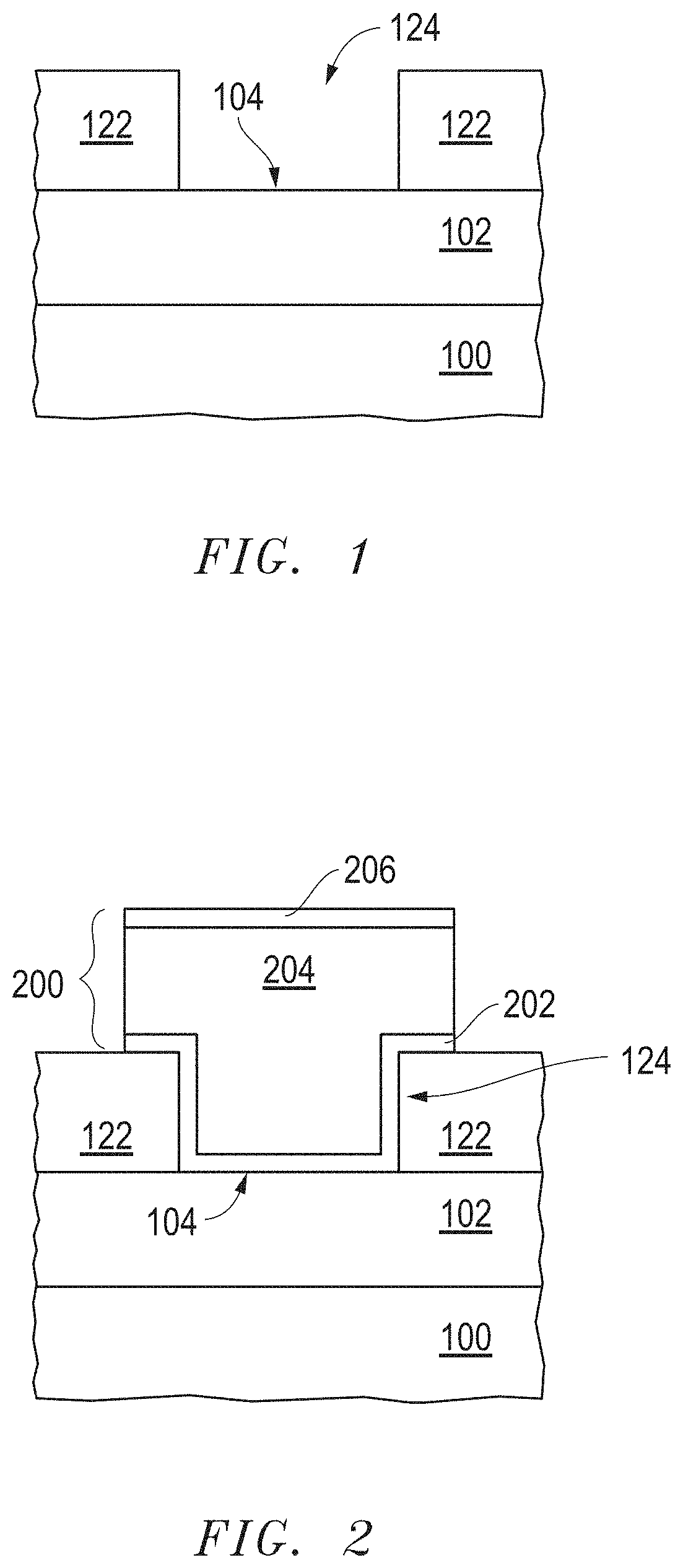
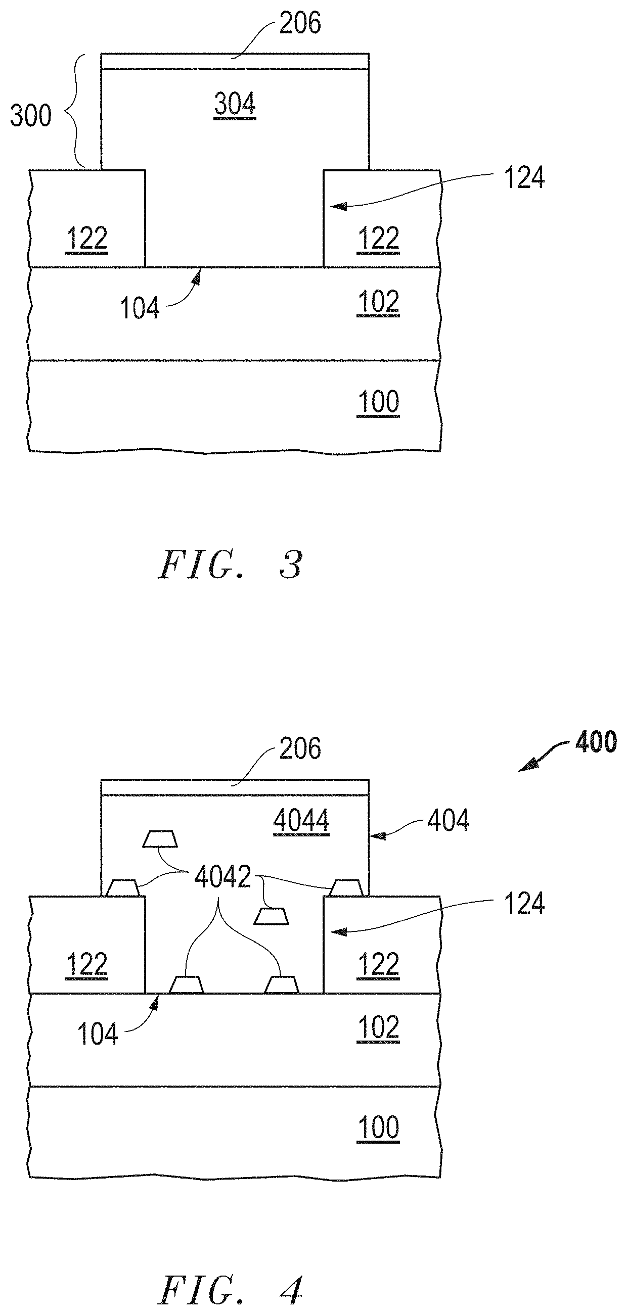
[0114]An electronic device can include a semiconductor layer and

[0115]a contact structure forming an ohmic contact with the semiconductor layer. The contact structure can include a first phase and a second phase different from the first phase, wherein the first phase includes Al, the second phase includes the metal, and the first phase contacts the semiconductor layer.

embodiment 2

[0116]The electronic device of Embodiment 1, wherein an interface between the semiconductor layer and the contact structure is free of an oxide.

embodiment 3

[0117]The electronic device of Embodiment 1, wherein the second phase includes Al3Me, Me2AlN, MeN, or a combination thereof, wherein Me is the metal.


PUM


Abstract

An electronic device can include a semiconductor layer and a contact structure forming an ohmic contact with the layer. In an embodiment, the semiconductor layer can include a III-N material, and the contact structure includes a first phase and a second phase, wherein the first phase includes Al, the second phase includes a metal, and the first phase contacts the semiconductor layer. In another embodiment, the semiconductor layer can be a monocrystalline layer having a surface along a crystal plane. The contact structure can include a polycrystalline material including crystals having surfaces that contact the surface of the monocrystalline layer, wherein a lattice mismatch between the surface of the monocrystalline layer and the surfaces of the crystals is at most 20%.

Description


Claims


Application Information

Patent Timeline
Owner SEMICON COMPONENTS IND LLC
Why Eureka
Try Eureka