Field effect transistor with reduced overlap capacitance
a field effect transistor and capacitance reduction technology, applied in the field of semiconductor structures, can solve the problems of adverse effect on device performance, and the second component of overlap capacitance may still be substantial, and achieve the effect of reducing overlap capacitan
- Summary
- Abstract
- Description
- Claims
- Application Information
AI Technical Summary
Benefits of technology
Problems solved by technology
Method used
Image

Examples
first embodiment
[0110]The second exemplary semiconductor structure at a next processing step is shown in FIG. 9 and a magnified view of a dielectric liner is shown in FIG. 9A. A gate spacer 40 is formed by deposition of a dielectric material and an anisotropic etch, such as a reactive ion etch, thereof in the same manner employed in the Exposed horizontal portions of the dielectric liner layer 38L is removed, for example, from above the disposable gate portion 24 and exposed surfaces of the semiconductor substrate 8 outside the area covered by the disposable gate portion 24 and the gate spacer 40. The remaining portion of the dielectric liner layer 38L constitutes a dielectric liner 38, which laterally surrounds the disposable gate portion 24, the metal gate portion 22, and the gate dielectric 20. The dielectric liner 38 is contiguous and of unitary construction, i.e., is in the form of one contiguous structure, and is topologically homeomorphic to a torus.
[0111]The dielectric liner 38 comprises a fi
third embodiment
[0122]Referring to FIG. 15, a third exemplary semiconductor structure according to the present invention is derived from the second exemplary semiconductor structure of FIG. 7 by forming a gate spacer 40′. The gate spacer 40′ is formed by deposition of a dielectric material and an anisotropic etch, such as a reactive ion etch, thereof. The deposition of the dielectric material is substantially conformal by selecting a process condition at which the reaction rate is substantially limited by temperature, and not be a reactant supply. Provided suitable deposition conditions are selected, low pressure chemical vapor deposition (LPCVD), plasma enhanced chemical vapor deposition (PECVD), high density plasma chemical vapor deposition (HDPCVD), or rapid thermal chemical vapor deposition (RTCVD) may be employed to effect a substantially conformal deposition of the dielectric material. No cavity is formed on the third exemplary semiconductor structure.
[0123]Referring to FIG. 16, a source region
second embodiment
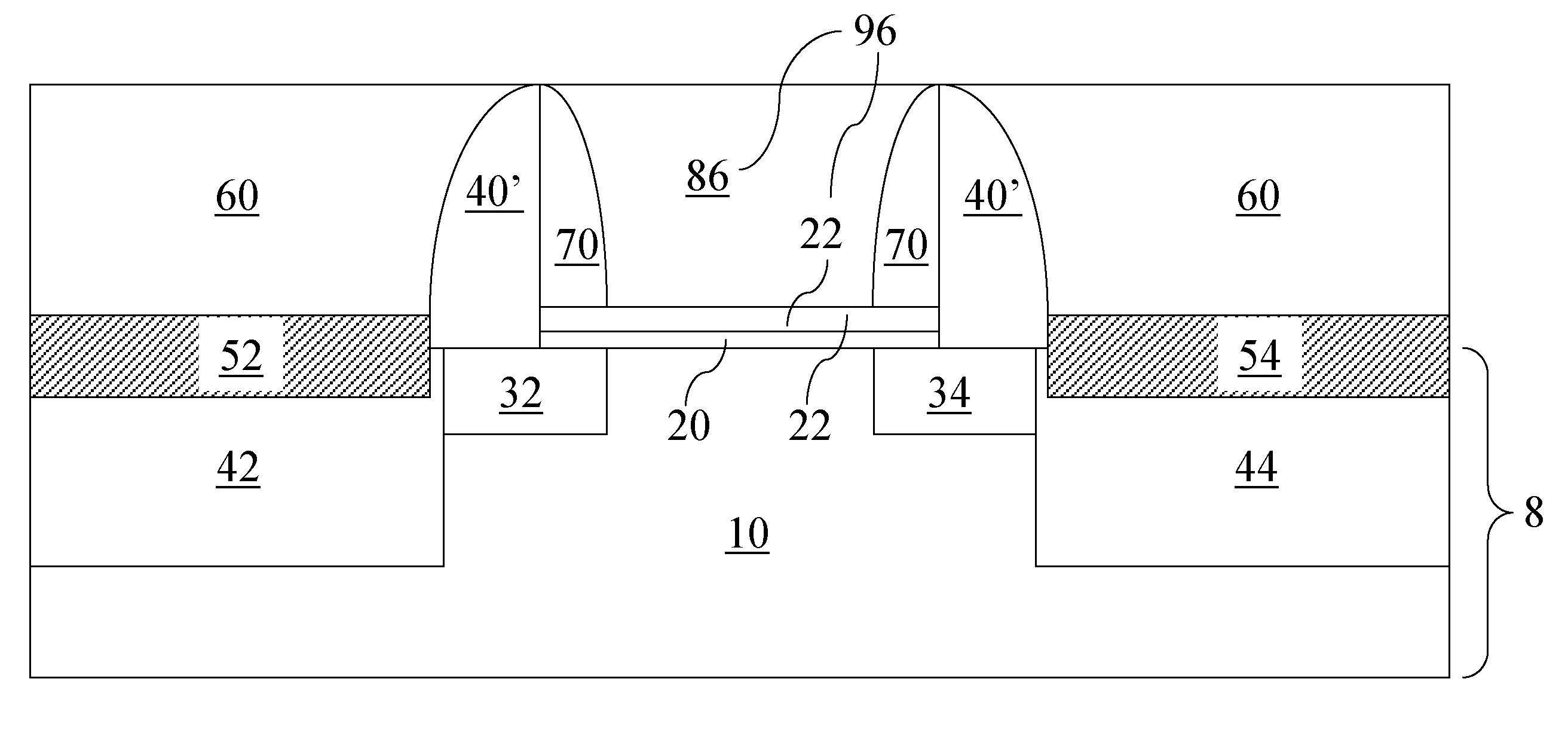
[0127]Referring to FIG. 20, a conductive gate portion 86 is formed directly on the metal gate portion 22 and the inner gate spacer 70 by deposition of a conductive material and planarization in the same manner as in the The conductive gate portion 86 and the metal gate portion 22 collectively constitute a gate electrode 96. The threshold voltage of the field effect transistor thus formed is determined by the work function of the metal gate portion 22 in addition to the dopant concentration, external stress, the material, and the crystallographic orientations of the semiconductor layer 11.
[0128]Due to the inner gate spacer 70, the distance between the source and drain extension regions (32, 34) and the conductive gate portion 86 is increased in comparison to prior art structures in which an inner gate spacer is not formed. Thus, the third exemplary semiconductor structure provides reduction in overlap capacitance between the gate electrode 96 and the source and drain extension regions
PUM
 Abstract
Description
Claims
Application Information
 - R&D Engineer
- R&D Manager
- IP Professional
- Industry Leading Data Capabilities
- Powerful AI technology
- Patent DNA Extraction
Browse by: Latest US Patents, China's latest patents, Technical Efficacy Thesaurus, Application Domain, Technology Topic.
© 2024 PatSnap. All rights reserved.Legal|Privacy policy|Modern Slavery Act Transparency Statement|Sitemap