Through-substrate vias and method of fabricating same
- Summary
- Abstract
- Description
- Claims
- Application Information
AI Technical Summary
Benefits of technology
Problems solved by technology
Method used
Image

Examples
Example
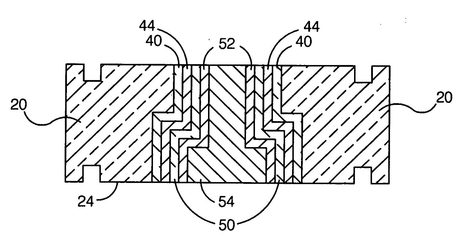
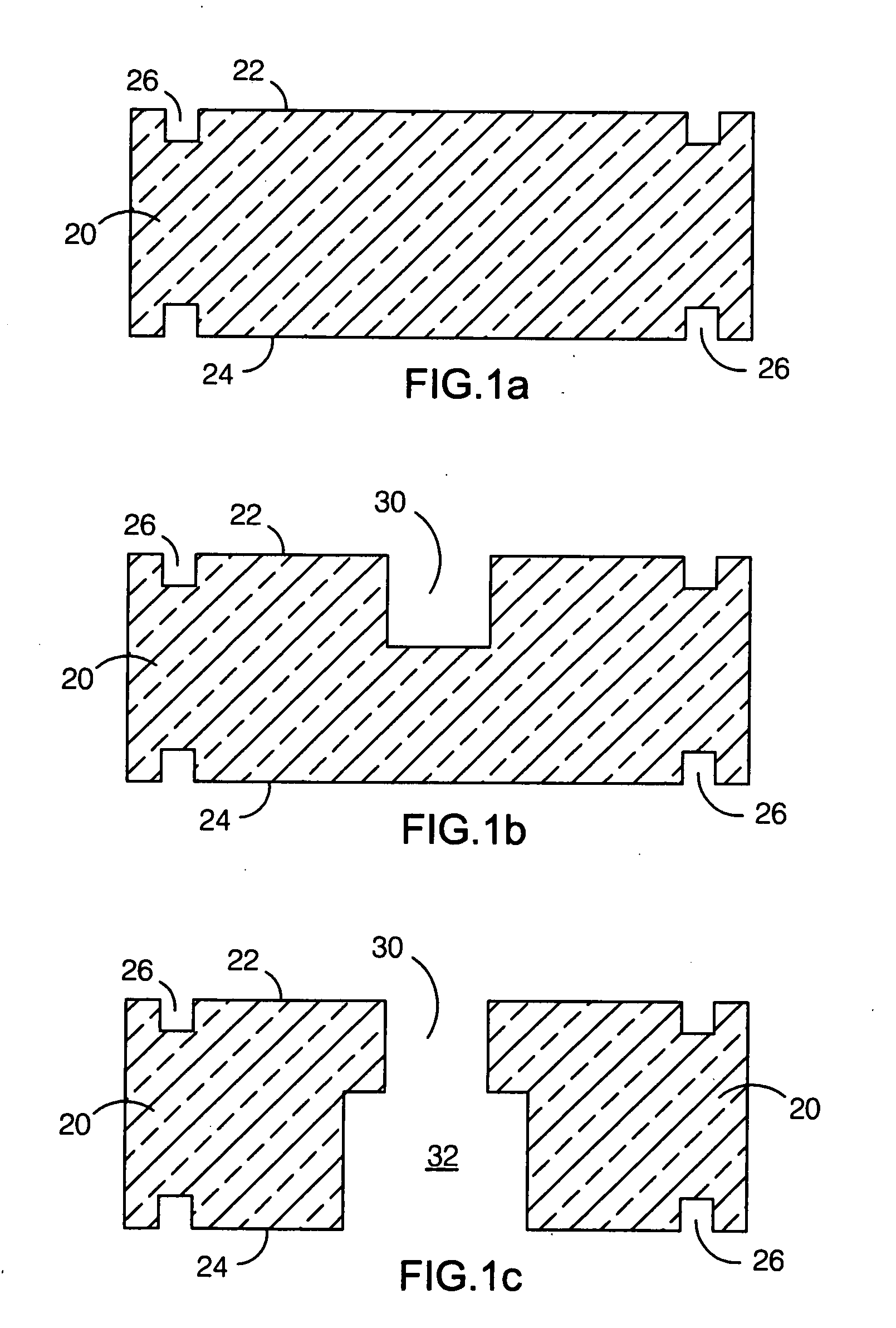
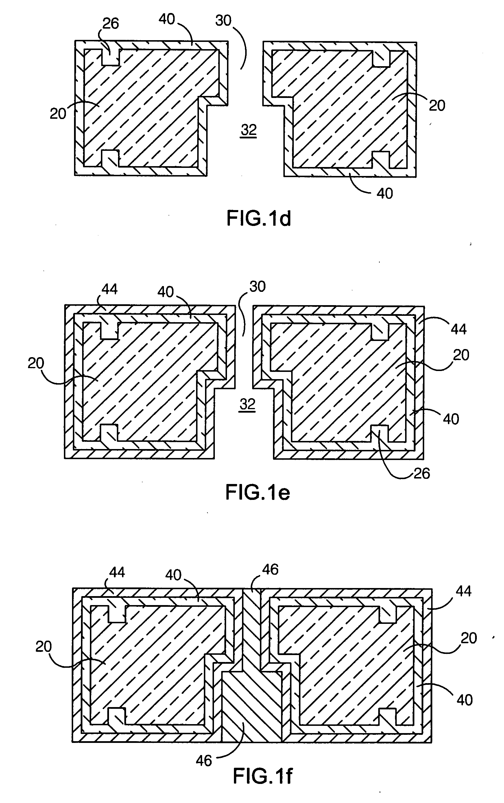
[0016]The present method is directed to a process for fabricating high aspect ratio through-substrate vias. The basic process steps are illustrated in the series of sectional views shown in FIGS. 1a-1g. In FIG. 1a, a substrate 20 has a first surface 22 and a second surface 24. Circuitry (not shown) may be disposed on first surface 22, on second surface 24, and / or between surfaces 22 and 24. The substrate may be made from any of a number of semiconductor materials, including but not limited to, silicon, gallium arsenide or indium phosphate. Alignment marks 26 may be etched on the first and second surfaces, to facilitate alignment of the substrate during subsequent process steps.
[0017]In FIG. 1b, a first cavity 30 is etched into first surface 22. The first cavity has a first diameter, and extends a first depth into the substrate. The first diameter is typically chosen to minimize the consumed circuit area on surface 22. The first depth is typically chosen to enable the first cavity to
PUM
 Abstract
Description
Claims
Application Information
 - R&D Engineer
- R&D Manager
- IP Professional
- Industry Leading Data Capabilities
- Powerful AI technology
- Patent DNA Extraction
Browse by: Latest US Patents, China's latest patents, Technical Efficacy Thesaurus, Application Domain, Technology Topic.
© 2024 PatSnap. All rights reserved.Legal|Privacy policy|Modern Slavery Act Transparency Statement|Sitemap