Physical quantity sensor, electronic device, and method of manufacturing physical quantity sensor

a technology of physical quantity sensor and electronic device, which is applied in the direction of electrical transducers, microstructural devices, instruments, etc., can solve the problems of poor area efficiency, increased chip area, and inferior resistance values to metals, and achieves low impedance and a lot of flexibility

Inactive Publication Date: 2011-05-19
SEIKO EPSON CORP
View PDF3 Cites 17 Cited by
  • Summary
  • Abstract
  • Description
  • Claims
  • Application Information

AI Technical Summary

Benefits of technology

The present invention provides an improved way for making sensors that can be customized by changing their placement on different types of electricity without being limited due to its flexible circuit design. This allows for more options when creating these devices while maintaining good performance over time.

Problems solved by technology

This patented describes how a type of electronic component called SRAM or MOSFET sensors use a special kind of crystal called Silicon Layer which allows electricity to pass through without being blocked up due to its own properties like size limitations. However, this design requires two layers: One needs to keep certain areas between them while another has more space than needed. To address these issues, proposes various methods including embedding static elec troads into SiO2/silic_oxy

Method used


Image

  • Physical quantity sensor, electronic device, and method of manufacturing physical quantity sensor
  • Physical quantity sensor, electronic device, and method of manufacturing physical quantity sensor
  • Physical quantity sensor, electronic device, and method of manufacturing physical quantity sensor

Examples


first embodiment

Overall Configuration of Capacitive Acceleration Sensor

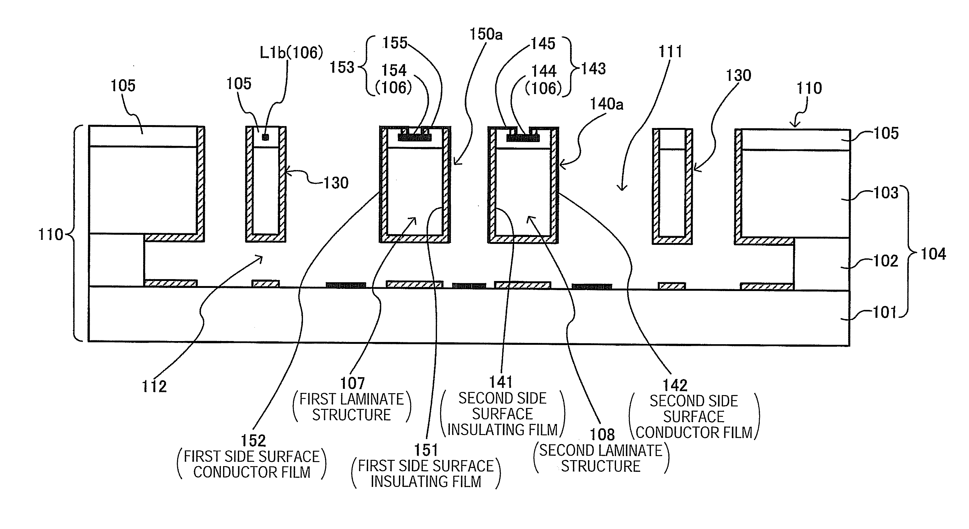
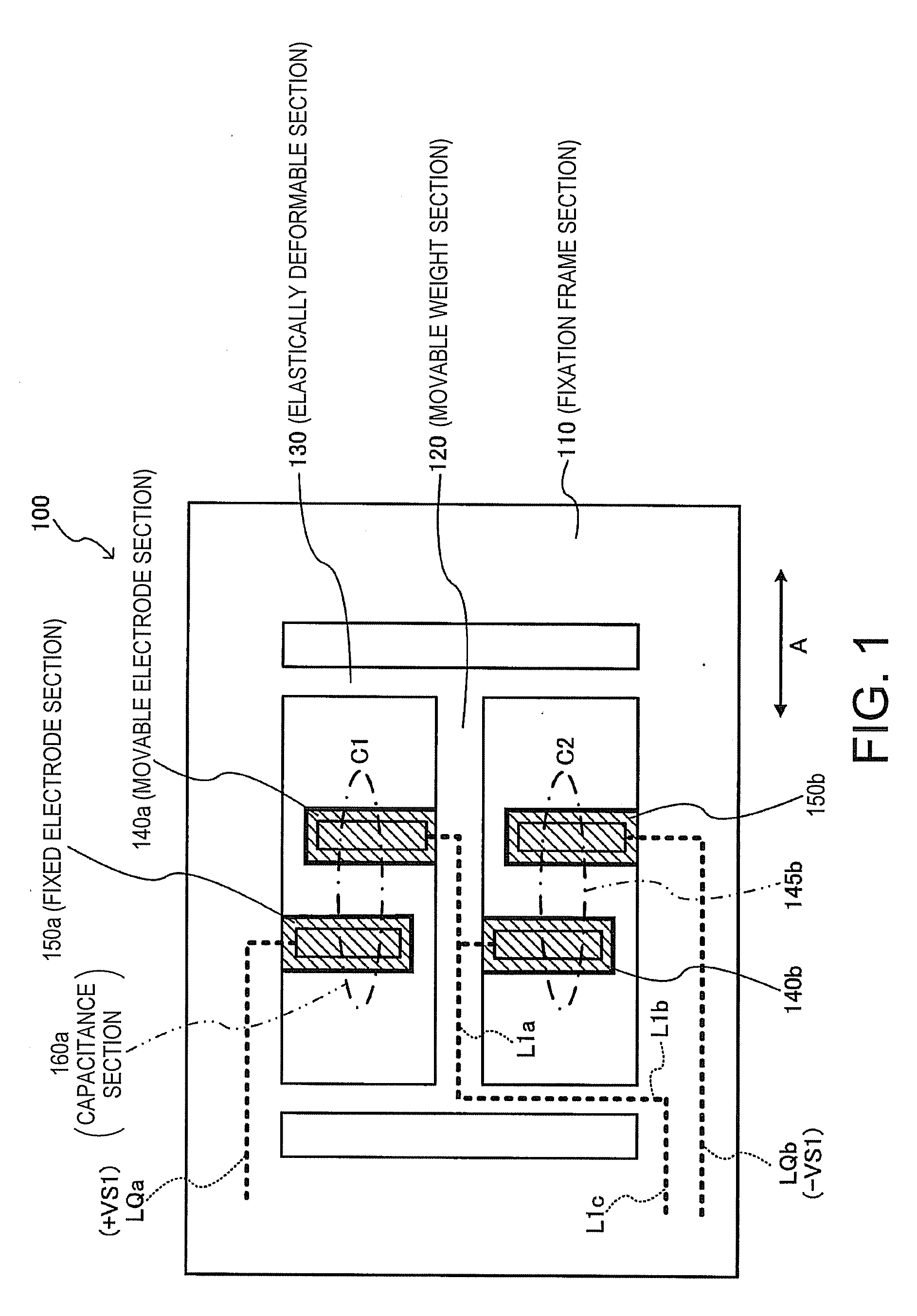
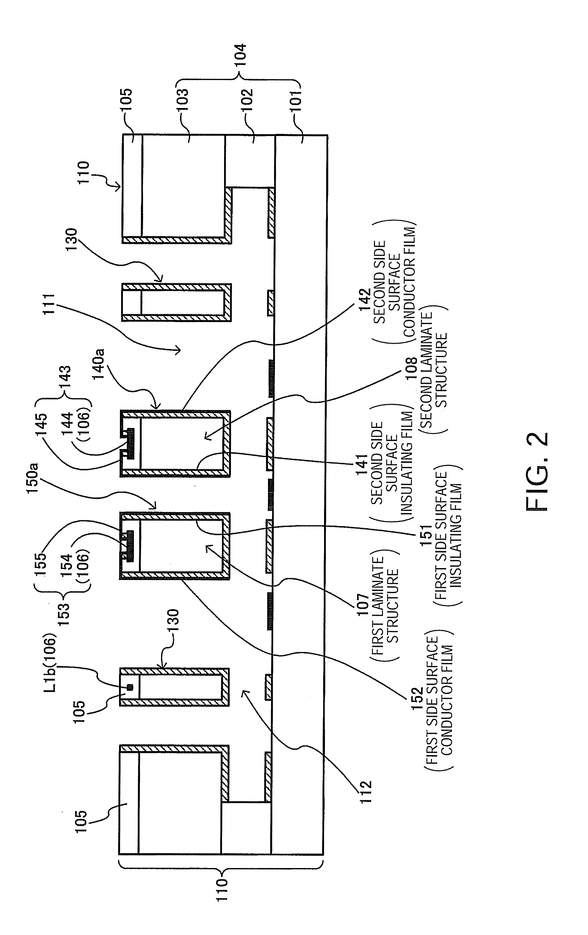
[0054]FIG. 1 is a plan view showing a configuration of an example (assumed here to be a capacitive acceleration sensor) of a MEMS sensor as a physical quantity sensor according to an embodiment of the invention. FIG. 2 is a cross-sectional view of the capacitive acceleration sensor shown in FIG. 1. FIG. 3 is a partial enlarged view of electrode sections 140, 150 shown in FIG. 2. It should be noted that the planar layout shown in FIG. 1 is illustrated as the simplest example, and in the present embodiment, the planar layout with high area efficiency shown in FIG. 13 can be adopted.

[0055]The capacitive acceleration sensor 100 shown in FIGS. 1 and 2 can be manufactured by forming a laminate structure on a substrate, and then selectively processing the laminate structure using a semiconductor manufacturing technology. For example, there can be used an SOI substrate 104 obtained by stacking an intermediate layer 102 (SiO2; referred also


PUM


Abstract

A physical quantity sensor includes: the fixed arm section includes a first side surface insulating film disposed on a side surface of the laminate structure, a first side surface conductor film disposed on a surface of the first side surface insulating film, and a first connection electrode section provided to the upper insulating layer, and electrically connected to the first side surface conductor film, the movable arm section includes a second side surface insulating film disposed on a side surface of the laminate structure, a second side surface conductor film disposed on a surface of the second side surface insulating film, and a second connection electrode section provided to the upper insulating layer, and electrically connected to the second side surface conductor film, and the first side surface conductor film and the second side surface conductor film are disposed so as to be opposed to each other.

Description


Claims


Application Information

Patent Timeline
Owner SEIKO EPSON CORP
Why Eureka
Try Eureka