Display apparatus and manufacturing method thereof

a technology of display apparatus and manufacturing method, which is applied in the direction of electrical apparatus, basic electric elements, and semiconductor devices, can solve the problems of constant power consumption of tft-lcd, low efficiency of modern oleds, and high power consumption of oleds, and achieves low power consumption, high efficiency, and high resolution

Active Publication Date: 2017-12-14
SEOUL SEMICONDUCTOR
View PDF9 Cites 76 Cited by
  • Summary
  • Abstract
  • Description
  • Claims
  • Application Information

AI Technical Summary

Benefits of technology

The present invention relates to an improved display device that uses small LEDs with very fine pixels for higher resolution, lower energy usage, and more efficient use compared to existing displays. This allows it to be used on various devices like smartphones or watches without being too bulky. Additionally, this design helps reduce the size of the device while still providing good performance.

Problems solved by technology

The technical problem addressed by this patent is how to reduce power consumption while maintaining good performance of OLED devices without compromising their effectiveness or causing issues with uniform brightness over time.

Method used


Image

  • Display apparatus and manufacturing method thereof
  • Display apparatus and manufacturing method thereof
  • Display apparatus and manufacturing method thereof

Examples


Embodiment Construction

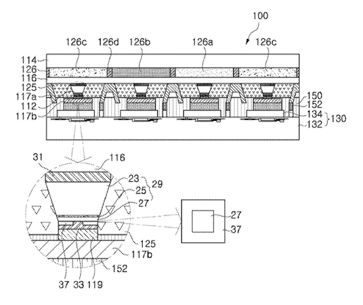
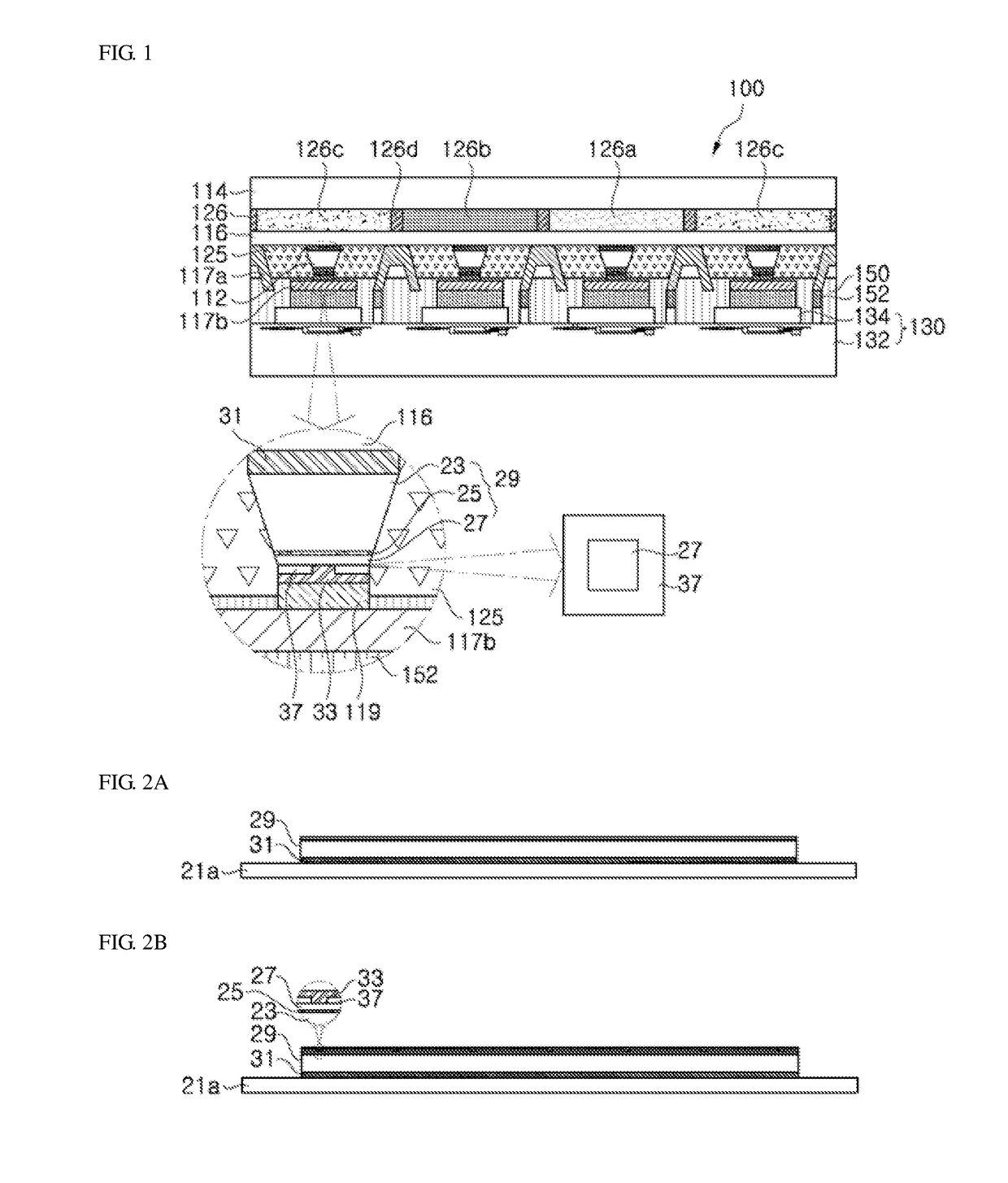
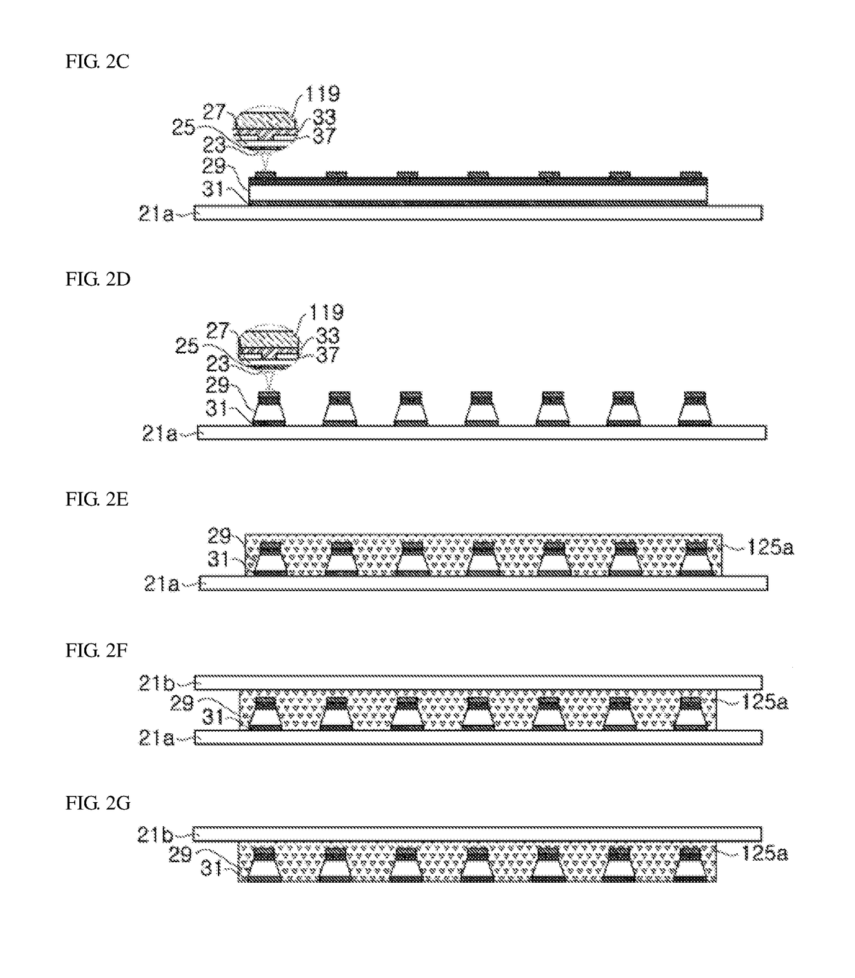
[0035]In the following description, for the purposes of explanation, numerous specific details are set forth in order to provide a thorough understanding of various exemplary embodiments. It is apparent, however, that various exemplary embodiments may be practiced without these specific details or with one or more equivalent arrangements. In other instances, well-known structures and devices are shown in block diagram form in order to avoid unnecessarily obscuring various exemplary embodiments.

[0036]In the accompanying figures, the size and relative sizes of layers, films, panels, regions, etc., may be exaggerated for clarity and descriptive purposes. Also, like reference numerals denote like elements.

[0037]When an element or layer is referred to as being “on,”“connected to,” or “coupled to” another element or layer, it may be directly on, connected to, or coupled to the other element or layer or intervening elements or layers may be present. When, however, an element or layer is refer


PUM


Abstract

A display apparatus including a light emitting diode part including a plurality of regularly arranged light emitting diodes, and a TFT panel part configured to drive the light emitting diode part. The light emitting diode part includes a transparent electrode, the light emitting diodes regularly disposed on a first surface of the transparent electrode and electrically connected to the transparent electrode, a plurality of first reflective electrodes disposed at sides of the light emitting diodes, surrounding the light emitting diodes, and electrically connected to the transparent electrode, and a plurality of second reflective electrodes electrically connected to the light emitting diodes, respectively, and reflecting light emitted from the light emitting diodes.

Description


Claims


Application Information

Patent Timeline
Owner SEOUL SEMICONDUCTOR
Why Eureka
Try Eureka