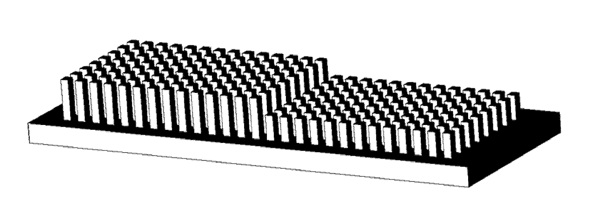
A microwave or millimeter wave RF part realized by die-forming

a technology of die-forming and microstrip lines, applied in waveguides, antennas, domestic articles, etc., can solve the problems of large losses in dielectric and conductive parts of microstrip networks, conductive losses are very high due to the miniaturization, and microstrip lines can only be made wider, so as to achieve cost-effective production and good performance

Active Publication Date: 2018-01-25
GAPWAVES
View PDF2 Cites 14 Cited by
  • Summary
  • Abstract
  • Description
  • Claims
  • Application Information

AI Technical Summary

Benefits of technology

The technical effect of this patented innovation relates to improving how waves are transmitted through materials used during signal transmissions between electronic devices such as radio transmitters (T) and receivers/transmitors). This improvement can be achieved by developing better ways to package these signals within smaller space while maintaining their quality level at higher frequencies like those found on 5G networks.

Problems solved by technology

Technological Problem addressed in this patents relates to improving electronic devices used in millimeter wavelength bands (650 nm-670nm) particularly those operating within 5G radiosets. Current solutions involve reducing impedance mismatch issues associated with microwave circuitry designs, including decreased signal quality caused by increased capacitant effects. To address this problem, researchers developed various techniques aiming towards improved design flexibility without compromising electrical properties. One approach involves embedding passively dampened grille patterns into certain areas inside the device housing itself, resulting in lesser inductor losses compared to traditional methods. Another solution includes creating smaller stubbing columns through a hole filled with a reflective material, allowing signals to escape while maintaining excellent radiofrequency characteristics.

Method used


Image

  • A microwave or millimeter wave RF part realized by die-forming
  • A microwave or millimeter wave RF part realized by die-forming
  • A microwave or millimeter wave RF part realized by die-forming

Examples


Embodiment Construction

[0096]In the following detailed description, preferred embodiments of the present invention will be described. However, it is to be understood that features of the different embodiments are exchangeable between the embodiments and may be combined in different ways, unless anything else is specifically indicated. Even though in the following description, numerous specific details are set forth to provide a more thorough understanding of e present invention, it will be apparent to one skilled in the art that the present invention may be practiced without these specific details. In other instances, well-known constructions or functions are not described in detail, so as not to obscure the present invention.

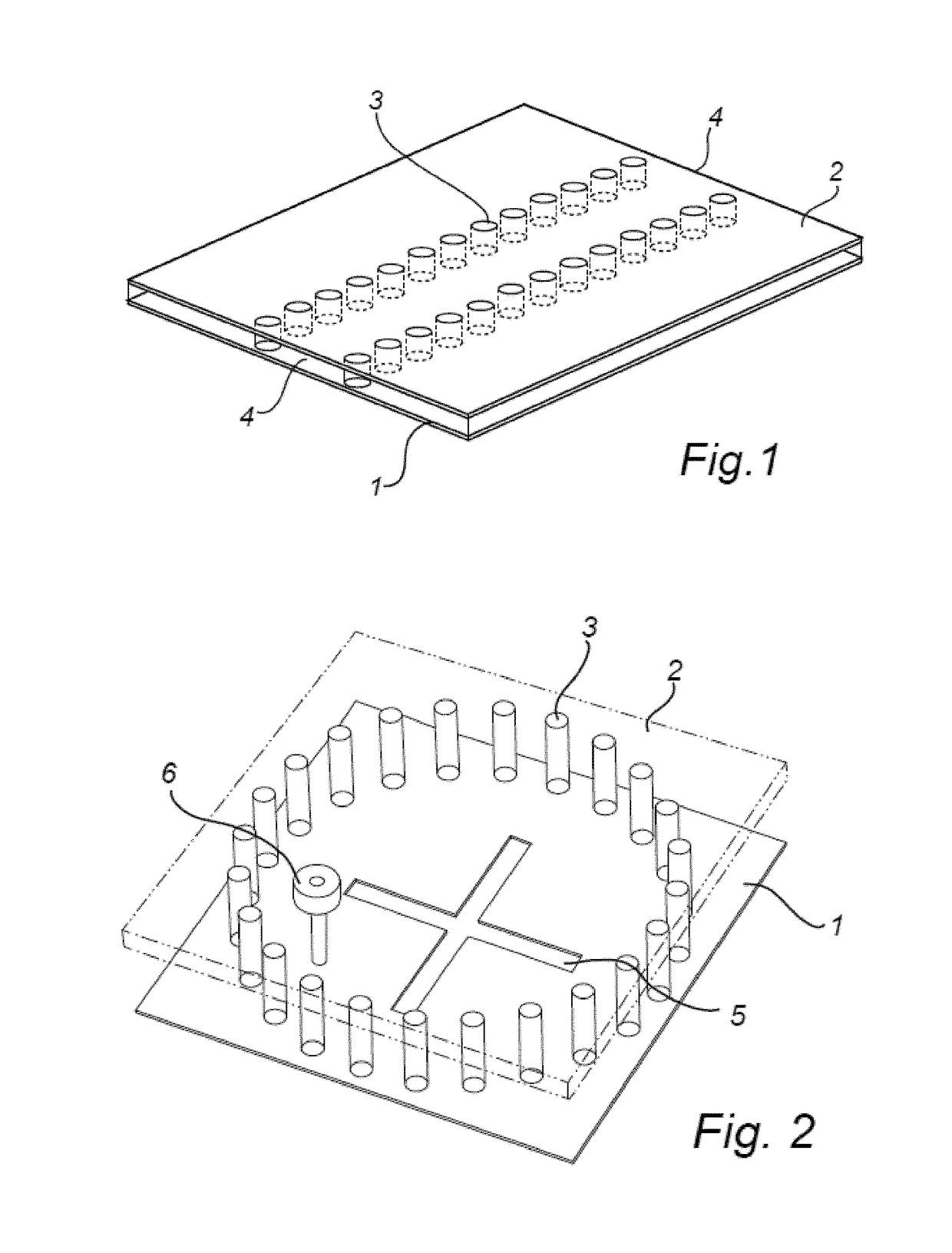
[0097]In a first embodiment, as illustrated in FIG. 1, an example of a rectangular waveguide is illustrated. The waveguide comprises a first conducting layer 1, and a second conducting layer 2 (here made semi-transparent, for increased visibility). The conducting layers are arranged at


PUM


Abstract

A method and apparatus for producing an RF part of an antenna system is disclosed, as well as thereby producible RF parts. The RF part has at least one surface provided with a plurality of protruding elements. In particular, the RF part may be a gap waveguide. The protruding elements are monolithically formed and fixed on a conducting layer, and all protruding elements are connected electrically to each other at their bases via the conductive layer. The RF part is produced by providing a die having a plurality of recessions forming the negative of the protruding elements of the RF part. The die may be a multilayer die, having several layers, at least some having through-holes to form the recessions. A formable piece of material is arranged on the die, and pressure is applied, thereby compressing the formable piece of material to conform with the recessions of the die.

Description


Claims


Application Information

Patent Timeline
Owner GAPWAVES
Why Eureka
Try Eureka