Fin cut profile using fin base liner

Active Publication Date: 2020-04-30
IBM CORP
View PDF5 Cites 0 Cited by
  • Summary
  • Abstract
  • Description
  • Claims
  • Application Information

AI Technical Summary

Problems solved by technology

The formation of the mask itself poses its own challenges, particularly in cutting mask fins to a consistent size.
Inconsistent mask sizes, for example resulting from an imperfect etch that leaves sloped mask walls, res

Method used


Image

  • Fin cut profile using fin base liner
  • Fin cut profile using fin base liner
  • Fin cut profile using fin base liner

Examples


Embodiment Construction

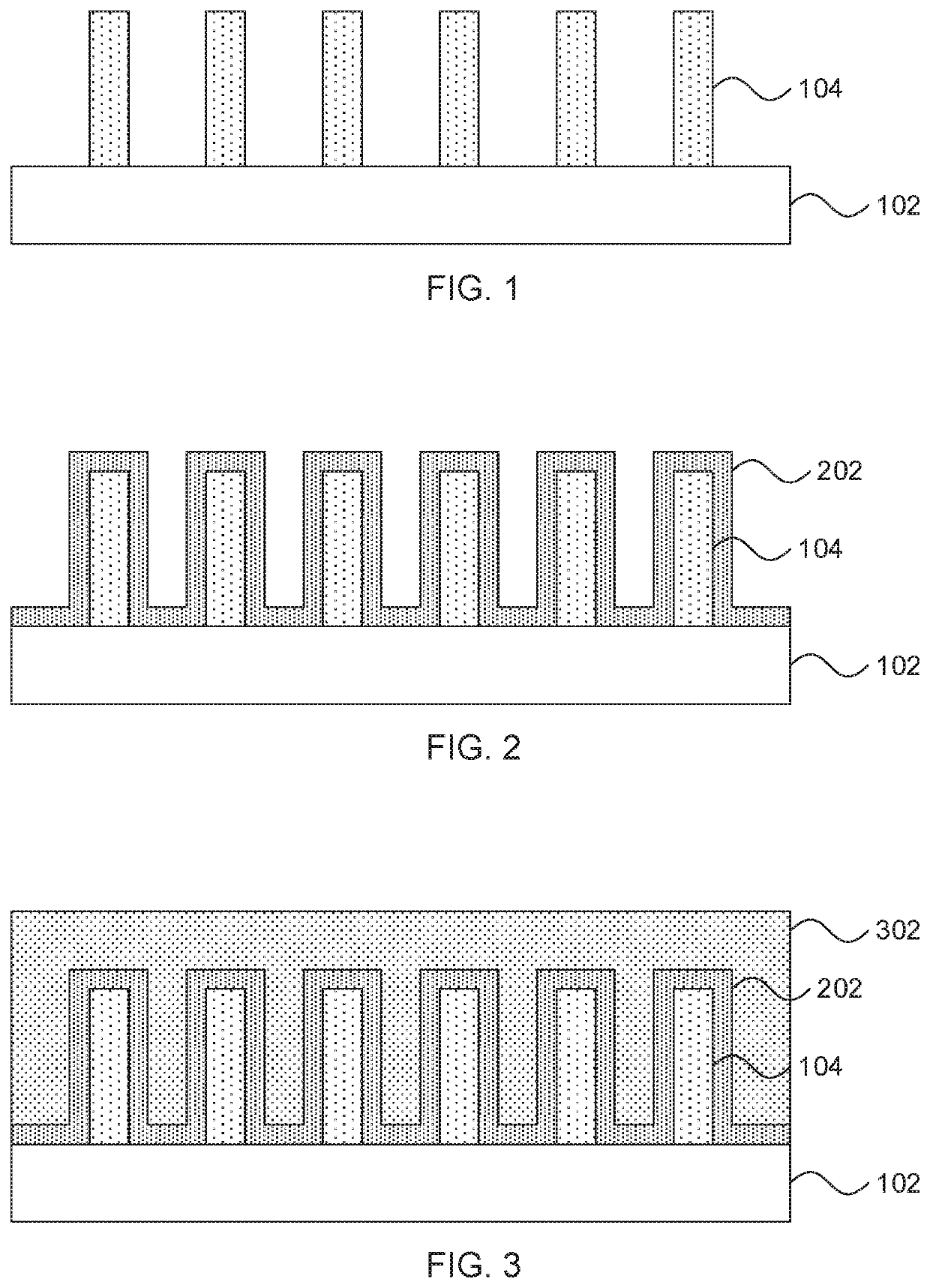
[0020]Embodiments of the present invention provide semiconductor devices that have superior fin length uniformity. This is accomplished by forming a protective liner at the base of the hardmask fins before cutting the hardmask fins to size. The protective liner enables the use of an etch chemistry that provides a superior hardmask fin profile without risking damage to the underlying semiconductor substrate.

[0021]Referring now to the drawings in which like numerals represent the same or similar elements and initially to FIG. 1, a cross-sectional view of a step in the formation of a set of semiconductor fins having sharp fin profiles is shown. A set of hardmask fins 104 is formed on a semiconductor layer 102. The composition of the hardmask fins 104 is shown herein as being a single layer of dielectric material, such as silicon nitride, but it should be understood that other compositions are contemplated, in particular fins formed from alternating layers of silicon oxide and silicon nitr


PUM


Abstract

Methods for forming semiconductor fins include forming a protective layer around a base of a hardmask fin on an underlying semiconductor layer. A portion of the hardmask fin is etched away with an etch that is selective to the protective layer. A semiconductor fin is etched from the semiconductor layer using the etched hardmask fin as a mask.

Description


Claims


Application Information

Patent Timeline
Owner IBM CORP
Why Eureka
Try Eureka