Semiconductor structure and forming method thereof

Active Publication Date: 2022-05-19
SEMICON MFG INT (SHANGHAI) CORP +1
View PDF2 Cites 0 Cited by
  • Summary
  • Abstract
  • Description
  • Claims
  • Application Information

AI Technical Summary

Problems solved by technology

However, the MP scaling is facing the challenges of a photolithography process limitation and an increased resistance, and due to device problems, the PP scaling has slowed down.
As the height of the

Method used


Image

  • Semiconductor structure and forming method thereof
  • Semiconductor structure and forming method thereof
  • Semiconductor structure and forming method thereof

Examples


Embodiment Construction

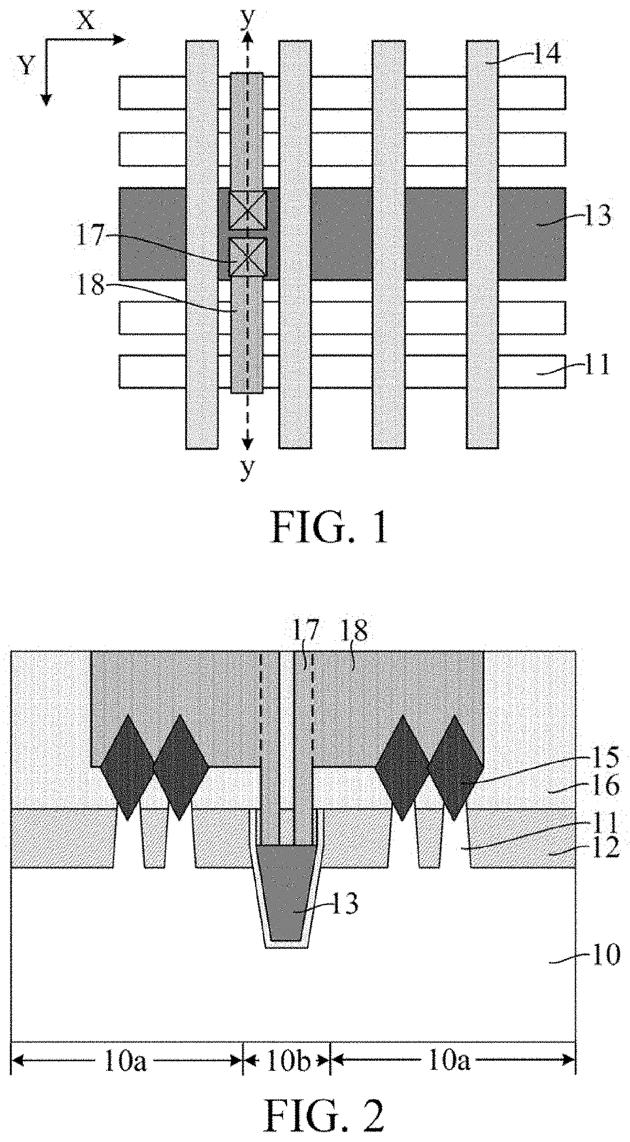
[0020]From the background, one of skill in the art will appreciate that a performance of a semiconductor device can be improved. A semiconductor structure is now combined to analyze the reasons why the performance of the device is still to be improved. FIG. 1 and FIG. 2 are schematic structural diagrams of a semiconductor structure. FIG. 1 is a top view, and FIG. 2 is a cross-sectional view of FIG. 1 in a y-y direction.

[0021]As shown in FIG. 1 and FIG. 2, the semiconductor structure includes: a substrate 10, including device regions 10a and a power rail region 10b; discrete fins 11 on the substrate 10 in the device regions 10a; an isolation structure 12, located on the substrate 10 exposed by the fin 11, where a top surface of the isolation structure 12 is lower than a top surface of the fin 11; a power rail line 13, located in the substrate 10 in the power rail region 10b and the isolation structure 12, where both the power rail line 13 and the fin 11 extend in a transverse direction


PUM


Abstract

A semiconductor structure and a forming method thereof are provided. In one form, a semiconductor structure includes: a substrate; discrete channel structures on the substrate in device regions; a power rail line, located in the substrate of a power rail region; a gate structure, extending across the channel structures; source/drain doped regions, located in the channel structures on two sides of the gate structure; an interlayer dielectric layer, located at a side portion of the gate structure; a power rail contact plug, penetrating a partial thickness of the interlayer dielectric layer at a top of the power rail line, where the power rail contact plug is in full contact with a top surface of the power rail line in a longitudinal direction; and a source/drain contact layer, located in the interlayer dielectric layer and in contact with the source/drain doped region, where on a projection surface parallel to the substrate, the source/drain contact layer extends across the power rail line. The power rail contact plug is in full contact with the top surface of the power rail line in the longitudinal direction, and a dimension of the power rail contact plug in the longitudinal direction and a contact area between the power rail contact plug and the power rail line are increased, to further help to reduce a resistance of the power rail contact plug and a contact resistance between the power rail line and the power rail contact plug.

Description


Claims


Application Information

Patent Timeline
Owner SEMICON MFG INT (SHANGHAI) CORP
Why Eureka
Try Eureka