Solid-state circuit assembly
A circuit device and semiconductor technology, which is applied in the manufacturing of semiconductor devices, circuits, and semiconductor/solid-state devices, etc., can solve problems such as the adverse effects of existing layout corrections and the decrease of integrated concentration.
- Summary
- Abstract
- Description
- Claims
- Application Information
AI Technical Summary
Problems solved by technology
Method used
Image

Examples
Embodiment Construction
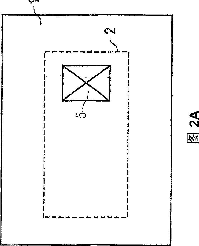
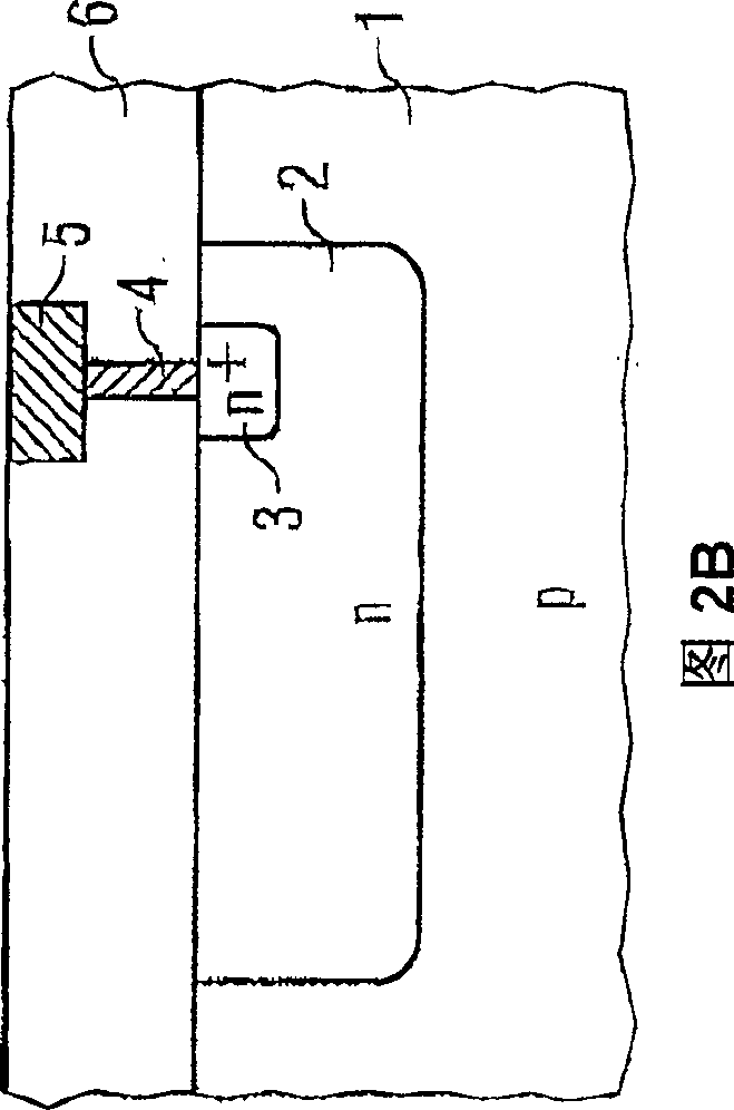
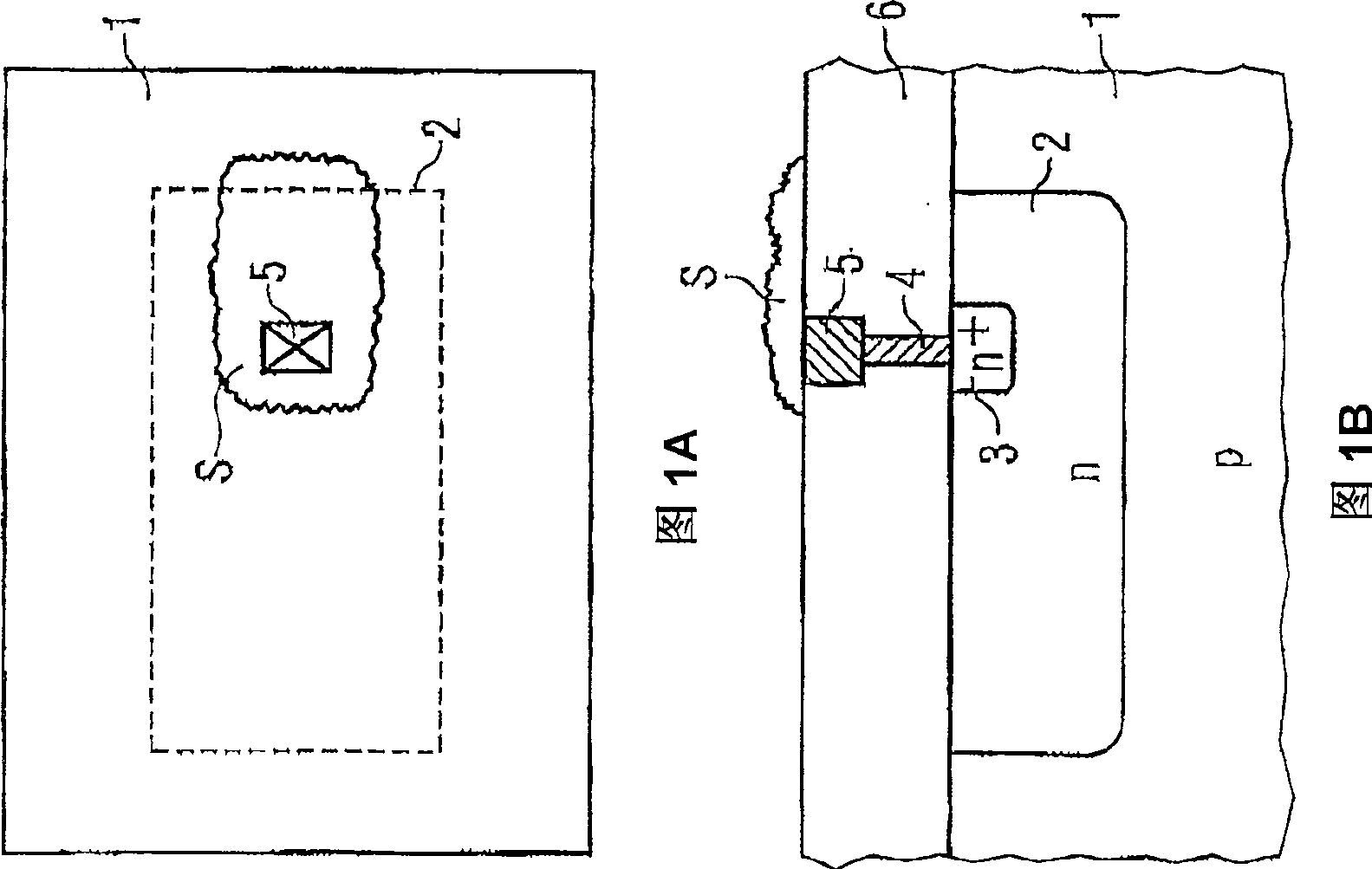
[0028] in accordance with Figure 3A and Figure 3B The semiconductor substrate 1 having at least one first doped region of the first conductivity type p also includes a second doped region 2 of the second conductivity type n opposite to the first conductivity type p. Furthermore, the highly doped connection doped region 3 of the second conductivity type n is sequentially placed in the second doped region 2 to connect this region, creating an ohmic junction with the second doped region 2 . The conductive structure to be planarized is at least partially embedded and one or more insulating layers 6 are formed on the surface of the semiconductor substrate 1 in contact with the connecting doped region 3 . The conductive structure in this example is a contact hole or aperture 4 that is filled with a conductive substance, and an interconnection layer 5 that is electronically connected thereto.
[0029] In order to implement the interconnection layer 5 , it is preferred to implement th
PUM
 Abstract
Description
Claims
Application Information
 - R&D Engineer
- R&D Manager
- IP Professional
- Industry Leading Data Capabilities
- Powerful AI technology
- Patent DNA Extraction
Browse by: Latest US Patents, China's latest patents, Technical Efficacy Thesaurus, Application Domain, Technology Topic.
© 2024 PatSnap. All rights reserved.Legal|Privacy policy|Modern Slavery Act Transparency Statement|Sitemap