Nano conductive ink and preparation method, RFID antenna and application thereof
A nano-conductive and ink technology, applied in antennas, applications, inks, etc., can solve the problems of ultra-thin, thick and high resistivity of RFID electronic tags that cannot be realized, improve compatibility and stability, reduce production costs, The effect of reducing thickness
- Summary
- Abstract
- Description
- Claims
- Application Information
AI Technical Summary
Benefits of technology
Problems solved by technology
Method used
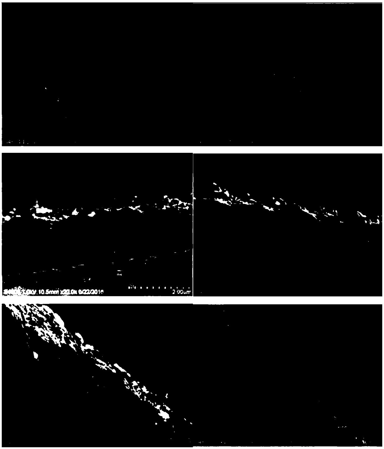
Image

Examples
Embodiment 1
[0038] A nano-conductive ink, comprising by weight: conductive metal filler, 60-80 parts; silver nanoparticles with a particle diameter of 2-50nm, 0.1-5 parts; polymer organic resin, 1-12 parts; adhesion promoter , 0.5-5 parts; leveling agent, 0.1-2 parts; defoamer, 0.1-2 parts; organic solvent, 10-25 parts.
[0039] Silver nanoparticles with a particle size of 2-50 nm start to melt at 90°C.
[0040] The conductive metal filler is any one of nano-level or micron-level silver powder, copper powder, and silver-coated copper powder, or any combination of several in any proportion.
[0041] The polymer organic resin is ethyl cellulose, hydroxypropyl cellulose, acrylic resin, polyurethane resin.
[0042] Adhesion promoter is any one of 928 adhesion promoter, acrylic acid, Tilcom IA 10; defoamer is any one of tributyl phosphate, polyoxypropylene glyceryl ether, polyoxyethylene polyoxypropanolamine ether The leveling agent is any one of isophorone, diacetone alcohol, and Solvesso150.
Embodiment 2
[0045] A kind of nano conductive ink, comprises by weight: conductive metal filler, 80 parts; Particle diameter is the silver nano particle of 2-50nm, 5 parts; High molecular organic resin, 12 parts; Adhesion promoter, 2.5 parts; Leveling Agent, 1 part; defoamer, 1 part; organic solvent, 18 parts. Others are the same as embodiment 1.
Embodiment 3
[0047] A nano-conductive ink, comprising by weight: conductive metal filler, 60 parts; silver nanoparticles with a particle diameter of 2-50nm, 0.1 part; polymer organic resin, 1 part; adhesion promoter, 0.5 part; leveling agent, 0.1 parts; defoamer, 2 parts; organic solvent, 25 parts. Others are the same as embodiment 1.
PUM
| Property | Measurement | Unit |
|---|---|---|
| Particle size | aaaaa | aaaaa |
| Particle size | aaaaa | aaaaa |
| Thickness | aaaaa | aaaaa |
Abstract
Description
Claims
Application Information
 - R&D Engineer
- R&D Manager
- IP Professional
- Industry Leading Data Capabilities
- Powerful AI technology
- Patent DNA Extraction
Browse by: Latest US Patents, China's latest patents, Technical Efficacy Thesaurus, Application Domain, Technology Topic.
© 2024 PatSnap. All rights reserved.Legal|Privacy policy|Modern Slavery Act Transparency Statement|Sitemap