Wafer treatment device
A technology for processing devices and wafers, used in electrical components, bearing components, semiconductor/solid-state device manufacturing, etc., can solve problems such as base wear, and achieve the effect of improving service life, increasing stability, and avoiding relative motion
- Summary
- Abstract
- Description
- Claims
- Application Information
AI Technical Summary
Problems solved by technology
Method used
Image

Examples
Example Embodiment
[0021] The specific embodiments of the wafer processing apparatus provided by the present invention will be described in detail below with reference to the accompanying drawings.
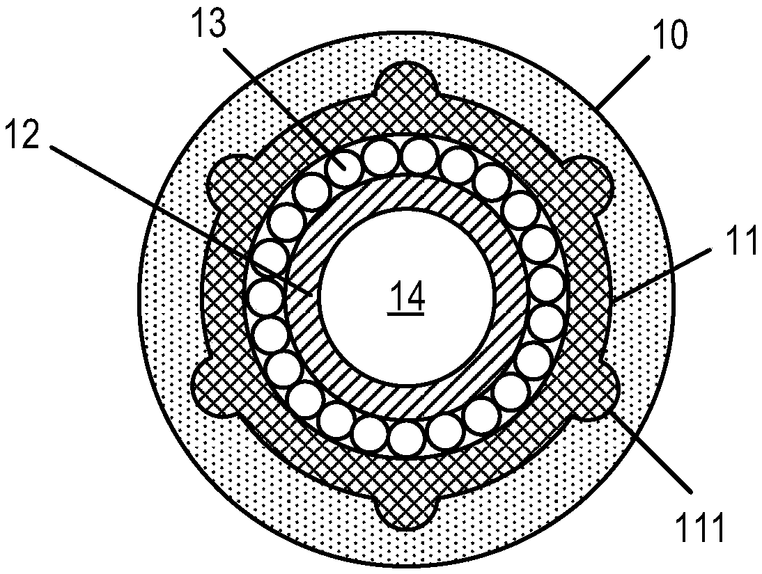
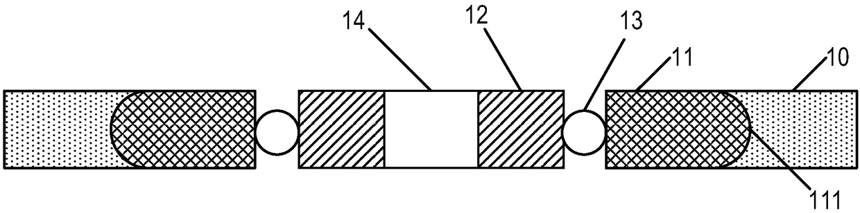
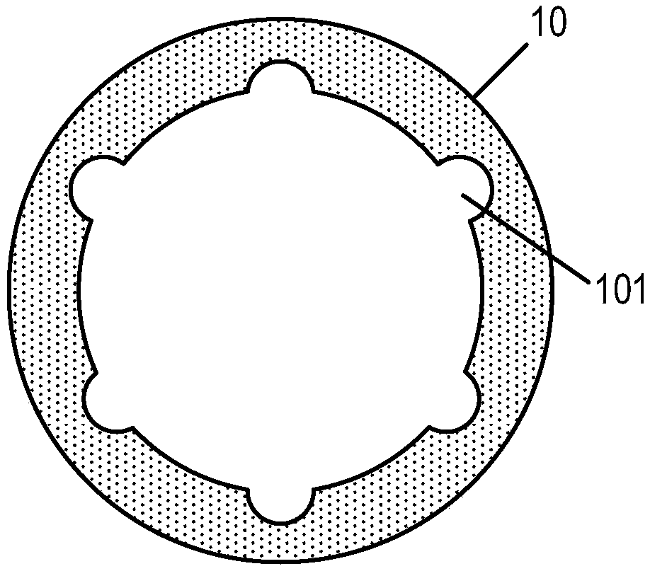
[0022] This specific embodiment provides a wafer processing apparatus, with figure 1 It is a top-view structural schematic diagram of a wafer processing apparatus in a specific embodiment of the present invention, with the attached figure 2 It is a schematic diagram of the cross-sectional structure of the wafer processing apparatus in the specific embodiment of the present invention. image 3 It is a schematic cross-sectional view of the base in the specific embodiment of the present invention.
[0023] like figure 1 , figure 2 , image 3 As shown, the wafer processing apparatus provided by this specific embodiment includes a base 10 for carrying wafers and a bearing nested in the base 10; the base 10 is in contact with the first bearing. The surface has a first connection structure, and the sec
PUM
 Abstract
Description
Claims
Application Information
 - R&D Engineer
- R&D Manager
- IP Professional
- Industry Leading Data Capabilities
- Powerful AI technology
- Patent DNA Extraction
Browse by: Latest US Patents, China's latest patents, Technical Efficacy Thesaurus, Application Domain, Technology Topic.
© 2024 PatSnap. All rights reserved.Legal|Privacy policy|Modern Slavery Act Transparency Statement|Sitemap