Manufacturing method of display panel

A manufacturing method and display panel technology, applied in semiconductor/solid-state device manufacturing, electrical components, electrical solid-state devices, etc., can solve problems such as failure and performance degradation, improve reliability, and solve the problem of sharp decline or even failure of TFT device performance Effect

Active Publication Date: 2019-12-31
HEFEI XINSHENG OPTOELECTRONICS TECH CO LTD +1
View PDF14 Cites 0 Cited by
  • Summary
  • Abstract
  • Description
  • Claims
  • Application Information

AI Technical Summary

Benefits of technology

The invention provides an improved method for creating layers on organic light-emitting devices (OLEDS). By adding specific materials like SiON2 instead of traditional fluoropolymers used during manufacturing processes, this process allows for better control over curing temperatures without affecting their effectiveness at lower temperatures. This results in more reliable display with fewer defects caused by poor quality components such as metal lines.

Problems solved by technology

This technical problem addressed in this patents relates to improving the quality control during manufacturing processes for making electronic displays with these types of display elements that have improved brightness levels over time without losing their functionality.

Method used


Image

  • Manufacturing method of display panel
  • Manufacturing method of display panel
  • Manufacturing method of display panel

Examples


Embodiment Construction

[0018] The application will be further described in detail below in conjunction with the accompanying drawings and embodiments. It should be understood that the specific embodiments described here are only used to explain related inventions, rather than to limit the invention. It should also be noted that, for ease of description, only parts related to the invention are shown in the drawings.

[0019] It should be noted that, in the case of no conflict, the embodiments in the present application and the features in the embodiments can be combined with each other. The present application will be described in detail below with reference to the accompanying drawings and embodiments.

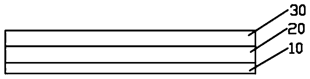
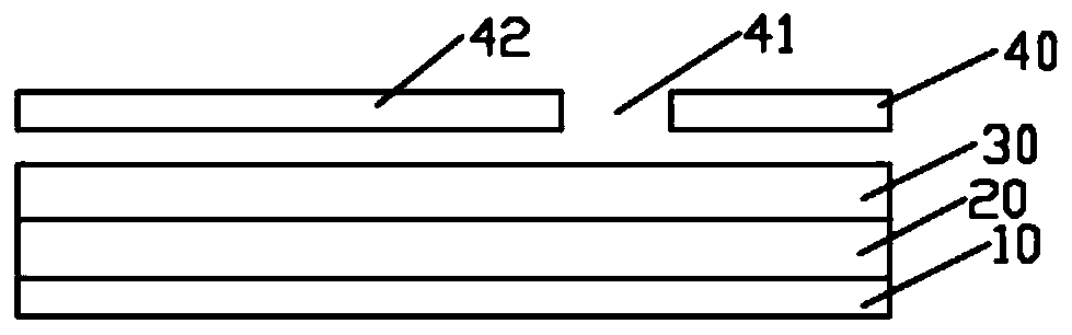
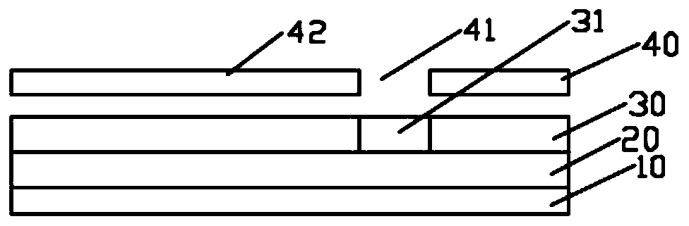
[0020] Please refer to Figure 1-4 , the manufacturing method of the display panel according to the embodiment of the present invention, comprising the following steps:

[0021] forming a thin film transistor layer 20 on the substrate 10;

[0022] A flat layer 30 is formed on the side of the thin f


PUM


Abstract

The invention discloses a manufacturing method of a display panel. The manufacturing method comprises the following steps: forming a thin film transistor layer on a substrate; forming a flat layer onthe side of the thin film transistor layer away from the substrate, wherein the material of the flat layer is siloxane; placing a mask plate at the position at a certain distance from the flat layer,performing ultraviolet irradiation on the local area of the flat layer through the mask plate and oxidizing the flat layer located in the local area; and performing dry etching on the flat layer to remove the oxidized flat layer located in the local area and enabling the thin film transistor layer to be exposed in the local area. The temperature is not higher than 200 DEG C in case of curing the flat layer, which will not cause sharp reduction of the performance of TFT devices or even failure, thus improving the reliability of OLED.

Description


Claims


Application Information

Patent Timeline
Owner HEFEI XINSHENG OPTOELECTRONICS TECH CO LTD
Why Eureka
Try Eureka