Two-port microstrip device testing device

A test device and two-port technology, applied in the direction of measuring devices, measuring device casings, components of electrical measuring instruments, etc., can solve problems such as device damage

Pending Publication Date: 2022-07-15
成都朗格微电科技有限公司
View PDF0 Cites 0 Cited by
  • Summary
  • Abstract
  • Description
  • Claims
  • Application Information

AI Technical Summary

Benefits of technology

The present in this new design allows for quicker and more efficient testings on small electronic components such as microswitch circuits or other types of circuitry that are difficult to access due to their size limitations. This technology makes it possible to perform tests while minimizing damage from heat during solder reflow processes.

Problems solved by technology

The technical problem addressed by this patented technology relates to improving the accuracy and efficiency of tests performed with two-port microwave devices (TMDs). Current methods require expensive equipment that may be damaged or cause harm during manufacturing processes due to their use.

Method used


Image

  • Two-port microstrip device testing device
  • Two-port microstrip device testing device
  • Two-port microstrip device testing device

Examples


Embodiment Construction

[0031] The present invention will be further described in detail below with reference to the examples, but the embodiments of the present invention are not limited thereto.

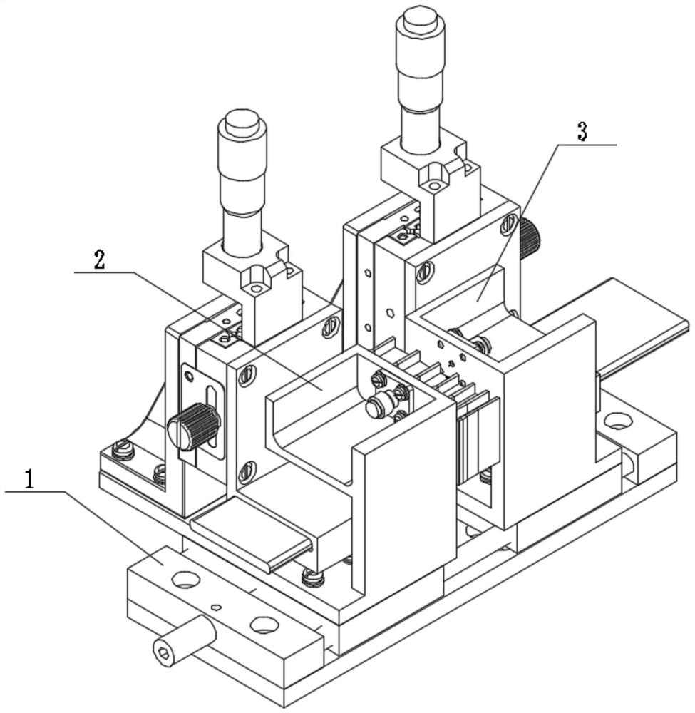
[0032] see Figure 1 to Figure 5 As shown, a two-port microstrip device testing device includes:

[0033] X-axis displacement platform 1;

[0034] The RF connector carrier A2 and the RF connector carrier B3 are arranged on the X-axis displacement platform 1, and the RF connector carrier A2 and the RF connector carrier B3 can move on the X-axis displacement platform 1 Move in the X direction.

[0035] The RF connector carrier A2 can be installed on one side of the X-axis displacement platform 1 by screws, and the RF connector carrier B3 can be installed on the other side of the X-axis displacement platform 1 by screws. The above structure mainly satisfies the movement of the radio frequency connector carrier A2 and the radio frequency connector carrier B3 in the X-axis direction.

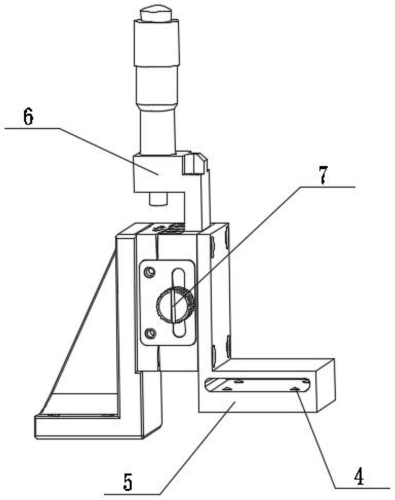
[0036] Z-axis displacem


PUM


Abstract

The invention discloses a two-port microstrip device testing device which comprises an X-axis displacement platform, a radio frequency connector carrying platform A, a radio frequency connector carrying platform B, a Z-axis displacement platform A, a Z-axis displacement platform B, an X-axis displacement platform, a bearing plate carrying platform A, a bearing plate carrying platform B, a bearing plate, ball spring screws and a to-be-tested piece carrying platform. Wherein the radio frequency connector platform deck A and the radio frequency connector platform deck B can move on the X-axis displacement platform along the X direction; ball spring screws are arranged in cavities of the bearing plate carrying table A and the bearing plate carrying table B and are positioned below the bearing plate; and the to-be-tested piece carrying table is positioned on the bearing plate between the radio frequency connector carrying table A and the radio frequency connector carrying table B. According to the invention, the device test can be rapidly and efficiently completed, and the connection of the microstrip line is completed by using a crimping method without welding and nondestructive test; moreover, the antenna is suitable for various microstrip line devices, and can be used in different lengths, different widths and different medium thicknesses.

Description


Claims


Application Information

Patent Timeline
Owner 成都朗格微电科技有限公司
Why Eureka
Try Eureka