Semiconductor device having electromagnetic wave absorbing layer with heat dissipating vias
a technology of electromagnetic wave absorption layer and heat dissipation via, which is applied in the direction of semiconductor/solid-state device details, cooling/ventilation/heating modification, semiconductor devices, etc., to achieve the effect of efficient dissipation of heat of semiconductor packages and high electromagnetic wave shielding properties
- Summary
- Abstract
- Description
- Claims
- Application Information
AI Technical Summary
Benefits of technology
Problems solved by technology
Method used
Image

Examples
first embodiment
A. First Embodiment
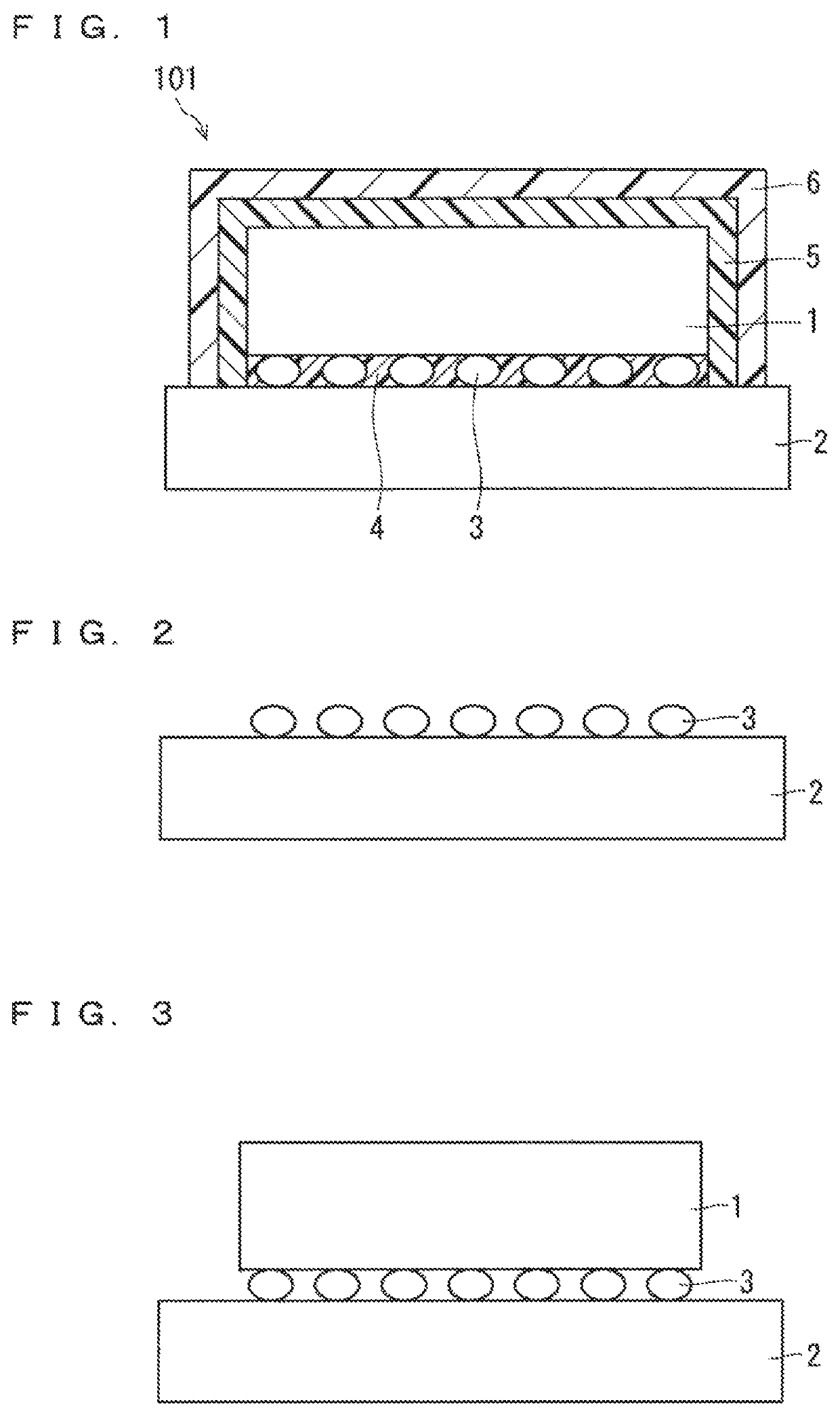
[0052]FIG. 1 is a cross-sectional view of a semiconductor device 101 according to a first embodiment of the present invention. In FIG. 1, the semiconductor device 101 includes a semiconductor package 1, a circuit board 2, solder 3, an underfill resin 4, an electromagnetic wave absorbing layer 5, and an electromagnetic wave reflecting layer 6. Herein, a semiconductor element that is composed of a silicon or compound semiconductor and is packaged with resin or the like is referred to as a semiconductor package. The semiconductor package 1 is, for example, an amplification IC or a high power module used in high frequency equipment.
[0053]The circuit board 2 is composed of a printed board made of glass epoxy resin and copper wiring, or alumina and silver wiring. Further, in a case where a multilayer board is used for the circuit board 2, the circuit board 2 may have a single patterned layer of Cu.
[0054]The semiconductor package 1 is bonded onto the circuit board 2 with th
second embodiment
B. Second Embodiment
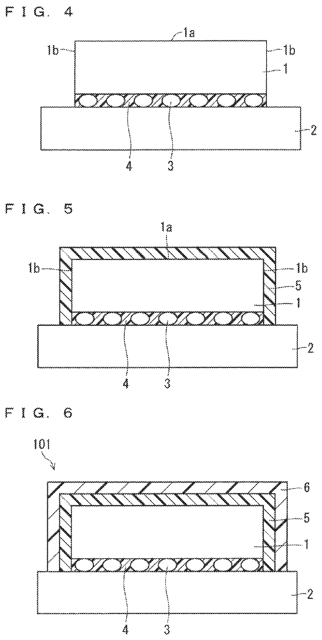
[0081]FIG. 9 is a cross-sectional view of a semiconductor device 102 according to a second embodiment of the present invention. The semiconductor device 102 differs from the semiconductor device 101 according to the first embodiment in that the electromagnetic wave absorbing layer 5 has an opening 51 on the upper surface of the semiconductor package 1, and a heat dissipating via 61 is formed in the opening 51. The heat dissipating via 61 is in contact with the electromagnetic wave reflecting layer 6 and the semiconductor package 1. Therefore, the electromagnetic wave reflecting layer 6 is in contact with the semiconductor package 1 via the heat dissipating via 61 in the opening 51 of the electromagnetic wave absorbing layer 5. Note that the opening 51 has a diameter of 0.1 mm, for example.
[0082]FIG. 10, FIG. 11, FIG. 12, and FIG. 13 are each a cross-sectional view of the semiconductor device 102, showing a first method for manufacturing the semiconductor device 102.
third embodiment
C. Third Embodiment
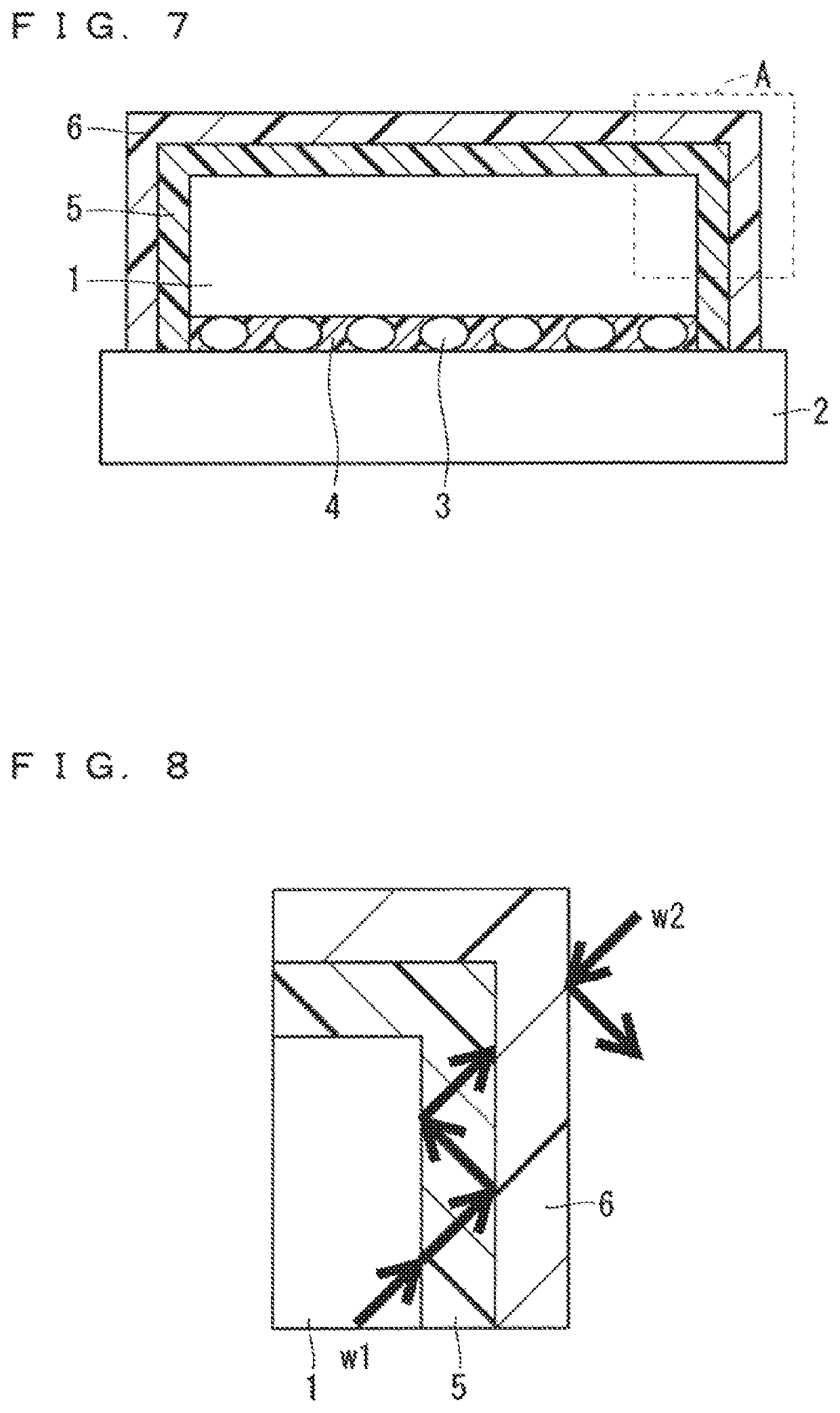
[0095]FIG. 18 is a cross-sectional view of a semiconductor device 103 according to a third embodiment of the present invention. The semiconductor device 103 differs from the semiconductor device 102 according to the second embodiment in that a metal film 7 is formed in the opening 51 of the electromagnetic wave absorbing layer 5, but is identical in other configurations to the semiconductor device 102.
[0096]The metal film 7 is in contact with the upper surface 1a of the semiconductor package 1 in the opening 51 of the electromagnetic wave absorbing layer 5. Further, the metal film 7 is less in thickness than the electromagnetic wave absorbing layer 5, and the heat dissipating via 61 is formed on the metal film 7 in the opening 51.
[0097]The metal film 7 is provided to increase heat transfer performance of a path extending from the semiconductor package 1 to the electromagnetic wave reflecting layer 6 via the heat dissipating via 61. The metal film 7 is made of metal h
PUM
 Abstract
Description
Claims
Application Information
 - R&D Engineer
- R&D Manager
- IP Professional
- Industry Leading Data Capabilities
- Powerful AI technology
- Patent DNA Extraction
Browse by: Latest US Patents, China's latest patents, Technical Efficacy Thesaurus, Application Domain, Technology Topic.
© 2024 PatSnap. All rights reserved.Legal|Privacy policy|Modern Slavery Act Transparency Statement|Sitemap