Wafer-level packaging method of semiconductor device
A wafer-level packaging and semiconductor technology, applied in the direction of semiconductor devices, electrical solid devices, electrical components, etc., can solve the problems of difficult packaging cost reduction, miniaturization, and breakthrough, so as to reduce thermal resistance and solve Reliability and heat dissipation issues, the effect of reducing production costs
- Summary
- Abstract
- Description
- Claims
- Application Information
AI Technical Summary
Benefits of technology
Problems solved by technology
Method used
Image

Examples
Embodiment 1
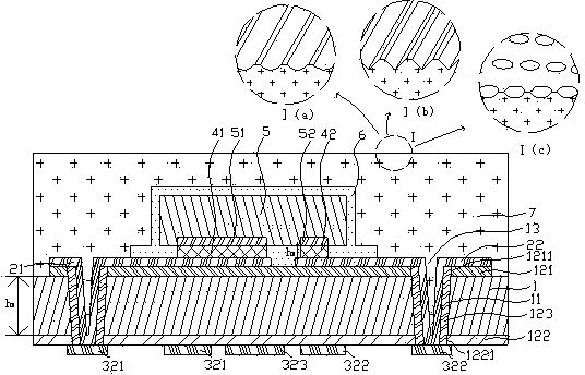
[0084] Example 1, see Figure 2-1 to Figure 2-10
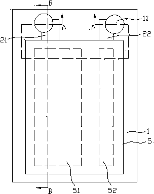
[0085] The packaging structure of semiconductor device LED such as Figure 2-2 with Figure 2-3 As shown, respectively diagram 2-1 A-A section view and B-B section view. An insulating layer I 121 is provided on the upper surface of the silicon-based substrate 1, and an insulating layer II 122 is provided on the lower surface. The material of the insulating layer I 121 and the insulating layer II 122 can be the same, and the material includes but not limited to silicon oxide film, so as to have semiconductor properties. The silicon-based substrate 1 is insulated. The upper surface of the insulating layer I121 is the rewiring metal layer pattern I21, the rewiring metal layer pattern II22, the rewiring metal layer pattern I21, and the rewiring metal layer pattern II22 that are insulated from each other. The material is generally made of metal copper, and its outermost layer It is a smooth and flat silver layer, aluminum layer (not sh
Embodiment 2
[0117] Such as Figure 3-1 to Figure 3-3 As shown, the difference between this embodiment and the first embodiment is:
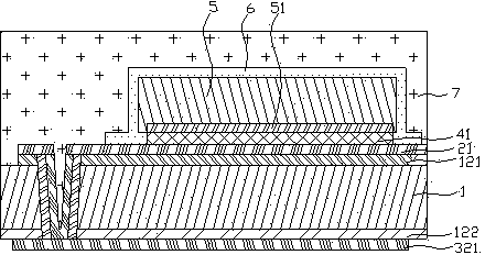
[0118] The positive electrode 51 and the negative electrode 52 of the LED chip 5 may respectively correspond to two through silicon vias 11, which are located outside the short ends of the positive electrode 51 and the negative electrode 52, such as Figure 3-1 with 3-2 Shown. The conductive electrode I321 and the conductive electrode II322 are distributed in parallel with the positive electrode 51 and the negative electrode 52, respectively cover the two through silicon holes 11 on the same side of the positive electrode 51 and the negative electrode 52, and are implemented with the positive electrode 51 and the negative electrode 52 on the same side. Electrical connection.
[0119] The positive electrode 51 and the negative electrode 52 of the LED chip 5 can respectively correspond to more than two through silicon vias 11, and the wiring metal layer pattern I21 an
Embodiment 3
[0122] Such as Figure 4-1 to Figure 4-5 As shown, the difference between this embodiment and the second and the third embodiment is:
[0123] The through silicon via 11 is arranged outside the long ends of the positive electrode 51 and the negative electrode 52, such as Pic 4-1 , Figure 4-2 Shown. The specific position of the through silicon via 11 outside the flip-chip area of the LED chip 5 is determined according to actual needs. The positive electrode 51 and the negative electrode 52 of the LED chip 5 can respectively correspond to two through silicon vias 11, and the rewiring metal layer pattern I21 and the rewiring metal layer pattern II22 can be back-to-back U-shaped to connect the two silicon through holes on the same side. Hole 11, two TSVs 11 can be arranged side by side, such as Figure 4-4 As shown, it can also be staggered. The conductive electrode I321 and the conductive electrode II322 are distributed in parallel with the positive electrode 51 and the negative e
PUM
| Property | Measurement | Unit |
|---|---|---|
| Thickness | aaaaa | aaaaa |
| Thickness | aaaaa | aaaaa |
| Thickness | aaaaa | aaaaa |
Abstract
Description
Claims
Application Information
 - R&D Engineer
- R&D Manager
- IP Professional
- Industry Leading Data Capabilities
- Powerful AI technology
- Patent DNA Extraction
Browse by: Latest US Patents, China's latest patents, Technical Efficacy Thesaurus, Application Domain, Technology Topic.
© 2024 PatSnap. All rights reserved.Legal|Privacy policy|Modern Slavery Act Transparency Statement|Sitemap