Double intracavity contacted long-wavelength VCSELs and method of fabricating same

a technology of vcsel and contact lens, which is applied in the direction of laser details, nanooptics, semiconductor lasers, etc., can solve the problems of poor electrical and thermal conductivity, certain limitations and drawbacks, and vcsel performan

Inactive Publication Date: 2002-02-28
RGT UNIV OF CALIFORNIA
View PDF0 Cites 4 Cited by
  • Summary
  • Abstract
  • Description
  • Claims
  • Application Information

AI Technical Summary

Benefits of technology

This patented technology allows for better performance at high temperatures with an Active Region that can be controlled through specific openings or windows on its surface. It also includes a way to make this area thinner without adding extra materials like In P instead of just making it too small.

Problems solved by technology

The technical problem addressed in this patented text relates to improves the efficiency and reliance of producing electronic devices called VC SELs while reducing costs and manufacturing time required. Current methods involve complex processes involving multiple steps including etching materials onto silica crystals before depositing other components. This limits production flexibility and reduces product quality due to variations caused during processing.

Method used


Image

  • Double intracavity contacted long-wavelength VCSELs and method of fabricating same
  • Double intracavity contacted long-wavelength VCSELs and method of fabricating same
  • Double intracavity contacted long-wavelength VCSELs and method of fabricating same

Examples


Embodiment Construction

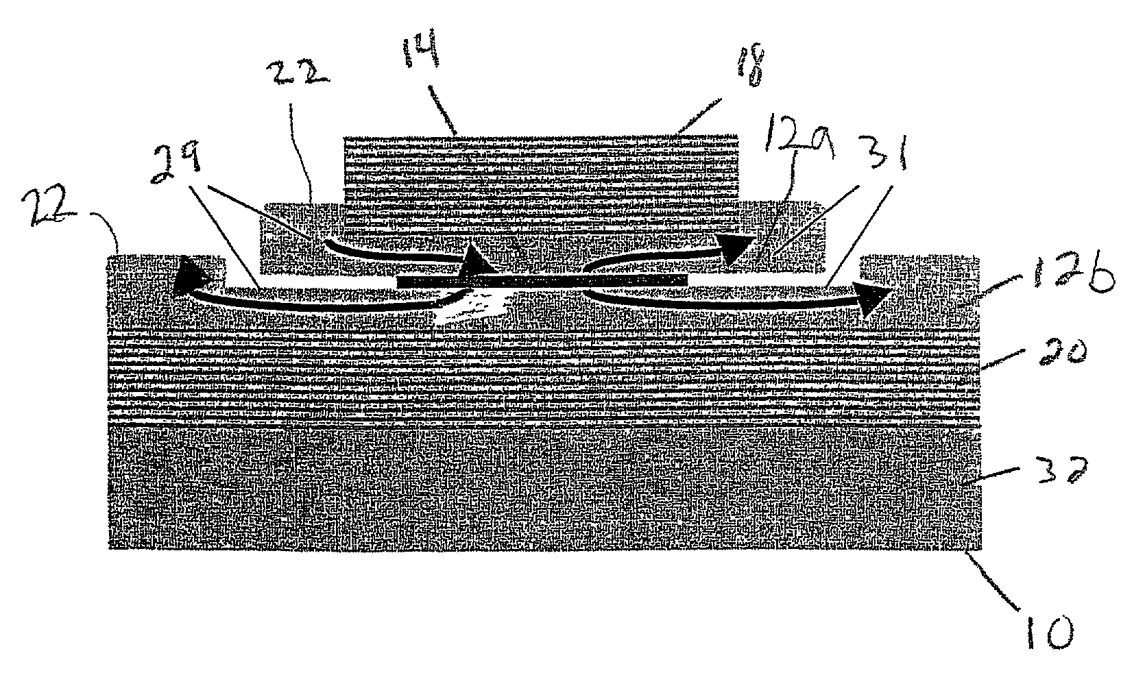
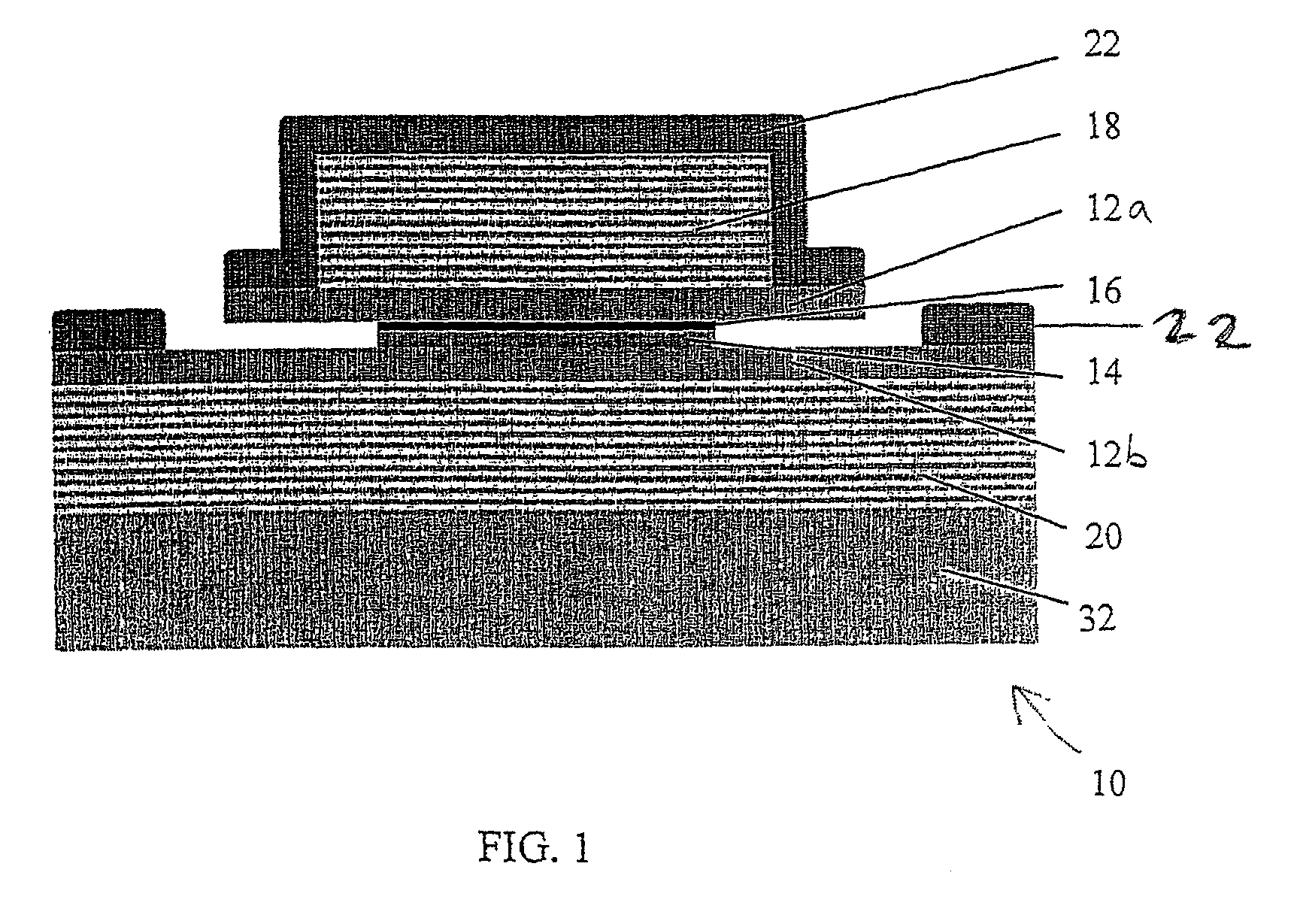
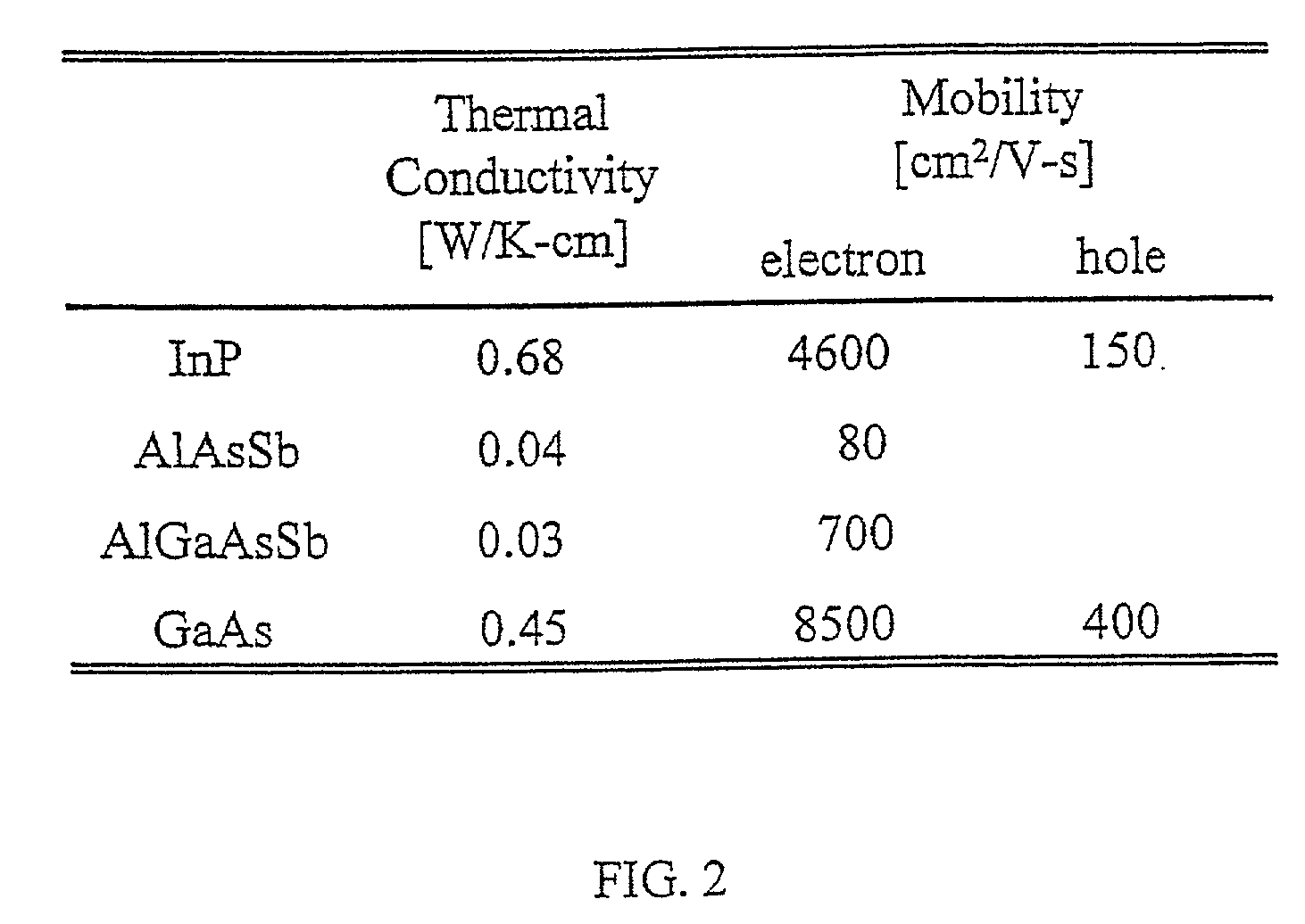
[0045] FIG. 1 is a schematic representation of a long wavelength VCSEL 10 having two InP layers 12a, 12b cladding an InAlGaAs-based active region 14, such that the active region 14 is disposed between the two InP layers 12a, 12b to form a double intracavity contacted structure. A tunnel junction 16 located between one of the InP layers 12a and the active region 14 generates holes for quantum wells in the active region 14 and allows both of the InP cladding layers 12a, 12b to be n-type. Only the InP cladding layers 12a, 12b, the tunnel junction 16 and part of the active region 14 are doped. Holes are created by the extraction of electrons from the valence band of a p-type layer in the tunnel junction 16. This design allows for the two n-type cladding layers 14 which have both higher electrical conductivity and lower optical loss than similarly-doped p-type layers. The tunnel junction 16 itself is at a standing-wave null of the cavity mode to minimize the absorption associated with the h


PUM


Abstract

A vertical cavity surface emitting laser (VCSEL) includes a semiconductor device having a pair of mirror portions, an active region, a tunnel junction, a pair of cladding layers and a substrate. Heat generated by the VCSEL dissipates through the cladding layers, which utilize an indium phosphide material. The VCSEL also includes selective etches that are used to aperture the active region to allow electric current to be injected into the active region.

Description


Claims


Application Information

Patent Timeline
Owner RGT UNIV OF CALIFORNIA
Why Eureka
Try Eureka