Array substrate, manufacturing method thereof and display device

A technology of an array substrate and a manufacturing method, which is applied in the display field, can solve problems such as difficulty in guaranteeing the quality of AMOLED display devices, complex process, superposition of production errors, etc., and achieve the effects of reducing production errors, simplifying process steps, and reducing the number of uses

Inactive Publication Date: 2014-10-08
BOE TECH GRP CO LTD
View PDF12 Cites 13 Cited by
  • Summary
  • Abstract
  • Description
  • Claims
  • Application Information

AI Technical Summary

Benefits of technology

This patented technology allows for efficient fabricating thin film transistors (TFTs) with improved performance compared to traditional methods such as photolithography or liquid crystal displays. It involves forming patterns directly onto the TFT' s material by means of lamination techniques that involve depositing layers over previously prepared areas without damaging them during subsequent processing. These new ways allow for more precise control over how electric current flows within each area covered by these layers while also reducing defect levels associated therewith. Overall, it makes better electronic devices possible due to faster operation speeds and reduced error rates caused by fewer maskings needed per step than previous technologies like LCD panels.

Problems solved by technology

This patented technical problem addressed in the patents relating to improving the performance of ActiveMatrix Liquid Crystalline Display Devices (AMLSD), specifically their use in mobile applications due to their lower costs compared to traditional technologies like Passively Addressed Memory Displays (PMANDM)). Current methods require complex multi-pattern processing techniques that result in continuously accumulated product error rates leading to reduced reliability and increased size requirements for these components.

Method used


Image

  • Array substrate, manufacturing method thereof and display device
  • Array substrate, manufacturing method thereof and display device
  • Array substrate, manufacturing method thereof and display device

Examples


Embodiment Construction

[0036] The following will clearly and completely describe the technical solutions in the embodiments of the present invention with reference to the accompanying drawings in the embodiments of the present invention. Obviously, the described embodiments are only some, not all, embodiments of the present invention. Based on the embodiments of the present invention, all other embodiments obtained by persons of ordinary skill in the art without making creative efforts belong to the protection scope of the present invention.

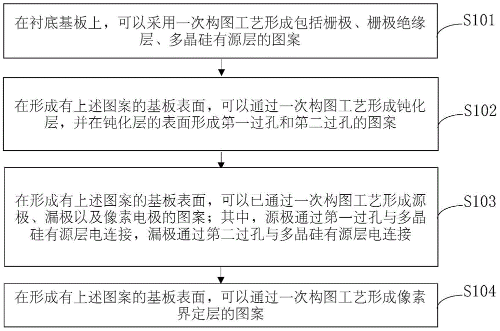
[0037] An embodiment of the present invention provides a method for manufacturing an array substrate, such as figure 2 As shown, can include:

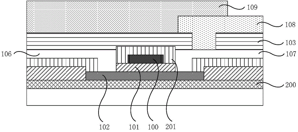
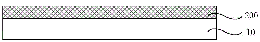
[0038] S101, in such as Figure 3d On the shown base substrate 10 , a pattern including a gate 100 , a gate insulating layer 101 , and a polysilicon active layer 102 can be formed by one patterning process.

[0039] S102, such as Figure 7b As shown, a passivation layer 103 may be formed on the surface of the substrat


PUM


Abstract

The embodiment of the invention provides an array substrate, a manufacturing method of the array substrate and a display device and relates to the technical field of display. The mask exposure technology using frequency is reduced in the low-temperature polycrystalline silicon AMOLED array substrate manufacturing process. In the array substrate manufacturing process, a grid, a gird insulating layer and a polycrystalline silicon active layer are formed on a substrate base plate through the one-time composition technology; then, patterns of a first via hole and a second via hole located in the surface of a passivation layer are formed through the one-time composition technology; next, a source, a drain and a pixel electrode are formed through the one-time composition technology, and the source and the drain are electrically connected with the polycrystalline silicon active layer through the first via hole and the second via hole respectively; finally, a pixel definition layer is formed through the one-time composition technology.

Description


Claims


Application Information

Patent Timeline
Owner BOE TECH GRP CO LTD
Why Eureka
Try Eureka