Semiconductor laser having protruding portion
a semiconductor and laser technology, applied in semiconductor lasers, semiconductor laser structural details, instruments, etc., can solve the problems of contact failure, unstable distance difficult to maintain a constant clearance between the side wall of the groove and the laser bar, so as to achieve less positional deviation, improve laser characteristic, and prevent undesirable spreading of the protective film on the end face
- Summary
- Abstract
- Description
- Claims
- Application Information
AI Technical Summary
Benefits of technology
Problems solved by technology
Method used
Image

Examples
embodiment 1
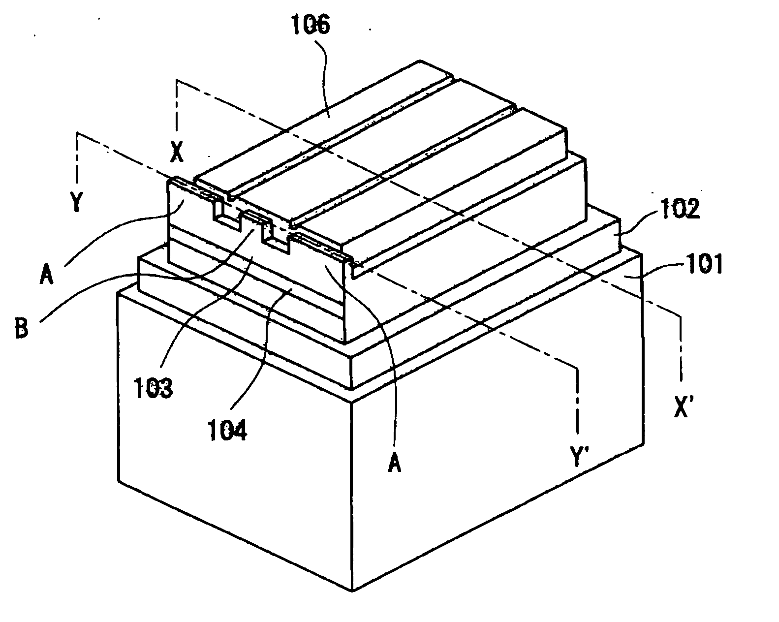
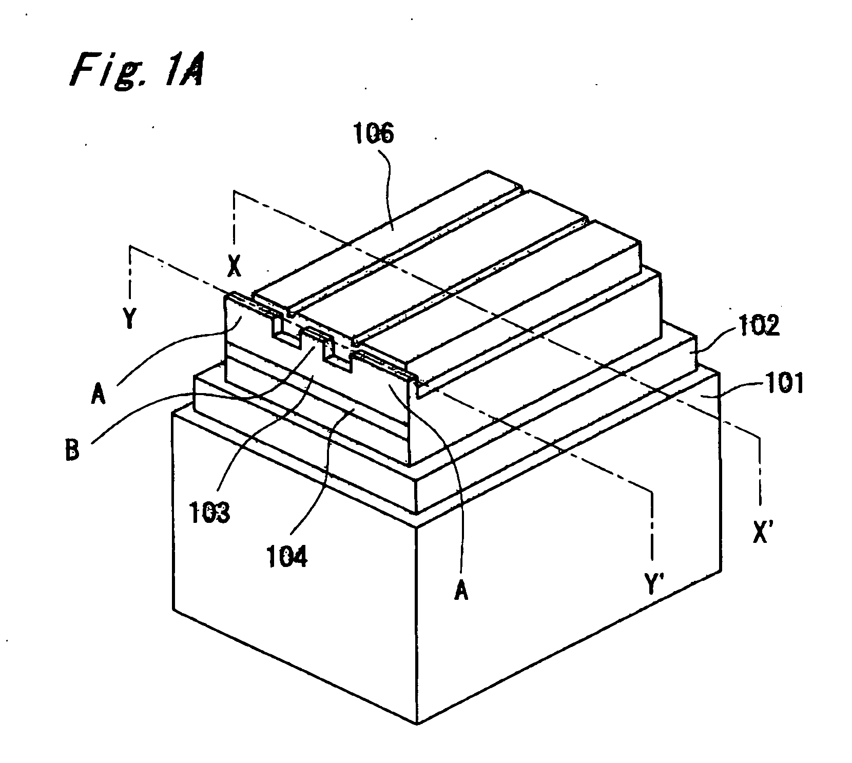
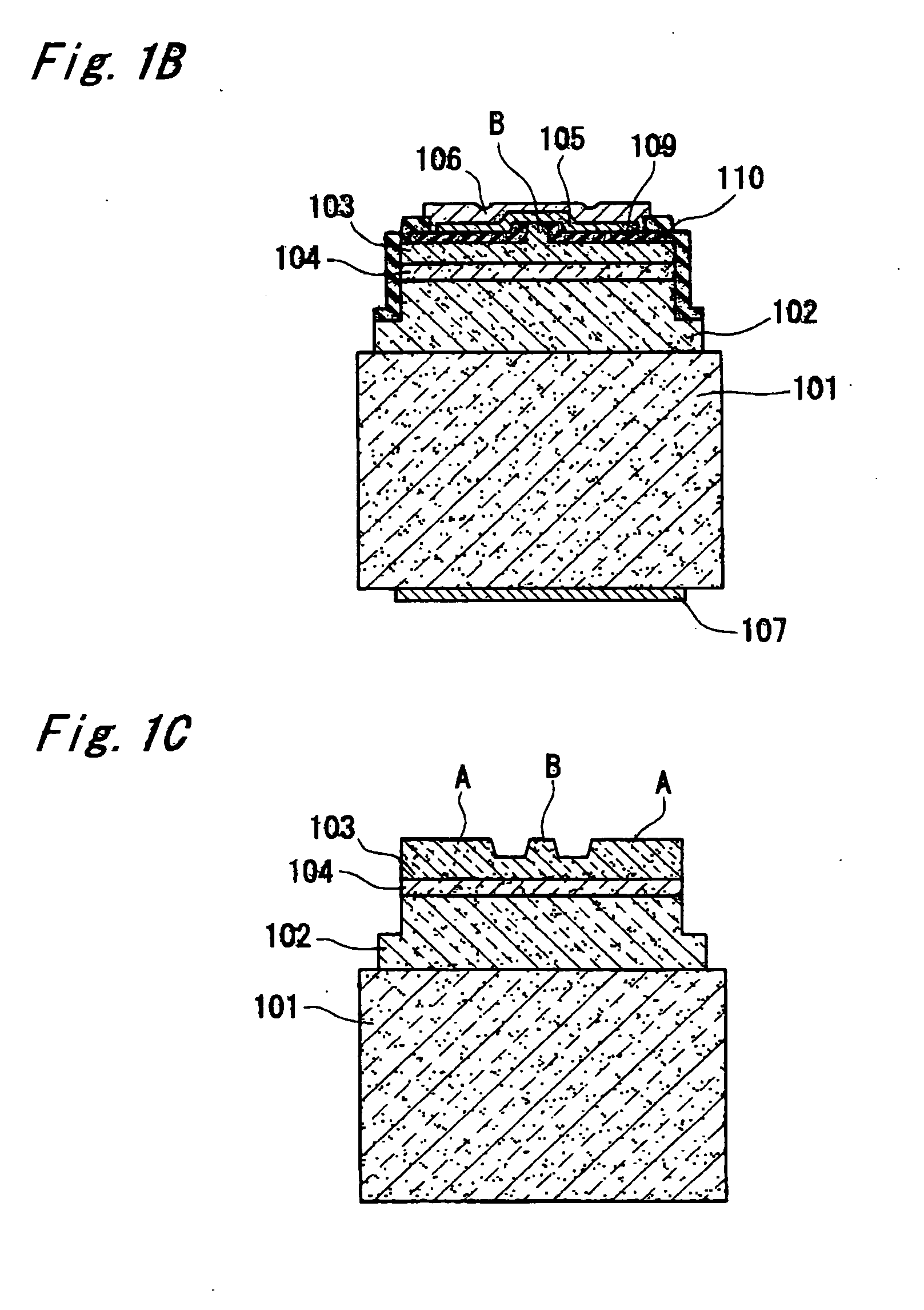
[0099] An example of forming a p-side protruding portion on a p-type semiconductor layer in this embodiment will be described. FIG. 1 is a schematic view showing the semiconductor laser device of this embodiment. FIG. 1B is a sectional view taken along lines XX′ in FIG. 1A. FIG. 1C is a sectional view taken along lines YY′ in FIG. 1A. The semiconductor laser device has an n-type semiconductor layer 102, an active layer 104 and a p-type semiconductor layer 103 stacked on a substrate 101, with a ridge B having stripe shape formed by etching a part of the p-type semiconductor layer. A first insulating film 109 is formed to extend from the side face of the ridge B onto the surface of the p-type semiconductor layer 103 on both sides of the ridge. A p-side ohmic electrode 105 is formed to extend from the surface of the ridge B onto the first insulating film 109. A p-side pad electrode 106 is formed on the p-side ohmic electrode 105. Portions of the surfaces of the p electrodes 105 and 106 ar
embodiment 2
[0111] This embodiment is an example of forming the n-side protruding portion A on the n-type semiconductor layer. FIGS. 2A through 2C schematically show the semiconductor laser device according to this embodiment. FIG. 2B is a sectional view taken along lines XX′ of FIG. 2A, and FIG. 2C is a sectional view taken along lines YY′ of FIG. 2A. This embodiment employs an insulating substrate 201 and, when the p electrode and the n electrode are formed on the same side of the substrate. Since the n-type semiconductor layer 12 is exposed by etching, the p electrode (p-side pad electrode) 206 and the n electrode (n-side pad electrode) 208 are different in the surface height as shown in FIG. 2B. As a result, a space is formed opening wide above the n electrode when forming the end face protective film as shown in FIG. 21B, thereby making it easier for the end face protective film to deposit on the n electrode. In this embodiment, in contrast, since the n-side protruding portion A is formed so
embodiment 3
[0147] This embodiment is an example where both the p-side protruding portion and the n-side protruding portion are formed. FIGS. 3A through 3C are schematic diagrams showing a form of the semiconductor laser device obtained according to the method of the present invention. FIG. 3B is a sectional view taken along lines XX′ of FIG. 3A, and FIG. 3B is a sectional view taken along lines YY′ of FIG. 3A. The protruding portions of p side and n side are provided as shown in FIG. 3. By providing the protruding portions of p side and n side, it is made possible to suppress the component of the end face protective film from depositing on the p electrode and the n electrode.
(P-Side Protruding Portion and N-Side Protruding Portion)
[0148] In order to suppress the component of the end face protective film from depositing on the electrodes, it is preferable to provide the protruding portions on both p side and n side as in this embodiment. If the protruding portion is to be provided on only one s
PUM
 Abstract
Description
Claims
Application Information
 - R&D Engineer
- R&D Manager
- IP Professional
- Industry Leading Data Capabilities
- Powerful AI technology
- Patent DNA Extraction
Browse by: Latest US Patents, China's latest patents, Technical Efficacy Thesaurus, Application Domain, Technology Topic.
© 2024 PatSnap. All rights reserved.Legal|Privacy policy|Modern Slavery Act Transparency Statement|Sitemap