Ion-sensitive thin film transistor for detecting ion activity of object to be detected and detection method
A thin-film transistor and ion-sensitive technology, which is applied in the field of semiconductor technology and intelligent detection, can solve the problems of insufficient development of ion sensors, and achieve the effect of simple structure, small size and good stability
- Summary
- Abstract
- Description
- Claims
- Application Information
AI Technical Summary
Benefits of technology
Problems solved by technology
Method used
Image

Examples
preparation example Construction
[0043] The present invention provides a kind of preparation method of above-mentioned ion sensitive thin film transistor, comprises the following steps:
[0044] (1) After forming a sensitive dielectric layer on the surface of the substrate, a patterned active layer is grown in the first region of the sensitive dielectric layer, and source and drain electrodes are grown at corresponding positions on the active layer; (2) in the sensitive dielectric layer A patterned second region is formed on the surface of the layer to obtain a device; (3) the device is packaged to obtain an ion-sensitive thin film transistor.
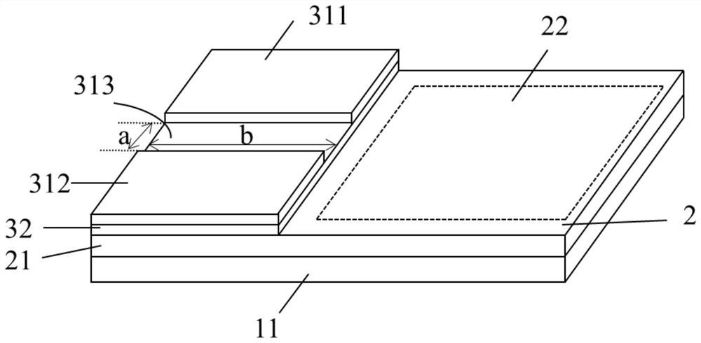
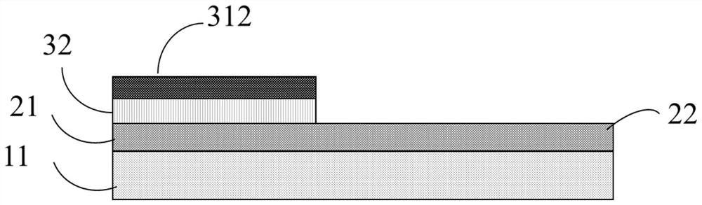
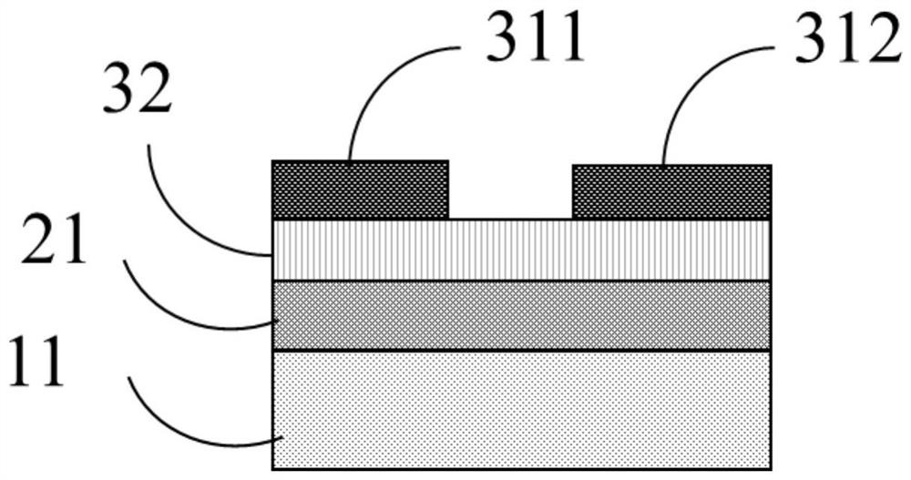
[0045] In step (1), the substrate is selected from a heavily doped substrate or a composite substrate, and when the substrate is a heavily doped substrate, such as figure 1 As shown, a sensitive dielectric layer 2 is sequentially formed on the surface of the heavily doped substrate 11, a patterned active layer 32 is grown on the first region 21 of the sensitive dielectri
Embodiment 1
[0059] Fabrication of Ion-Sensitive Thin Film Transistors
[0060] (1) Provide a silicon nitride substrate with a thickness of 60nm, use trimethylaluminum and water as precursors, and deposit Al with a thickness of 40nm on the substrate 2 o 3 The thin film is a sensitive dielectric layer, and the deposition temperature is 200°C;
[0061](2) Using diethylzinc and water as precursors, on the surface of the sensitive medium layer 2, glue coating, photolithography, deposition, development and degumming are carried out successively, so that the first region 21 of the sensitive medium layer 2 has a thickness of 40nm The ZnO thin film is the patterned active layer 32, wherein the deposition temperature is 200°C;
[0062] (3) Using gold as a raw material, the active layer 32 is sequentially coated with glue, photolithography, deposited, developed and stripped, so that a patterned source electrode 311 and drain electrode 312 are obtained on the active layer 32 to obtain a device , wher
Embodiment 2
[0067] Fabrication of Ion-Sensitive Thin Film Transistors
[0068] (1) A polyimide substrate is provided, and a metal layer with a thickness of 50nm is deposited on the polyimide substrate to obtain a composite substrate; with trimethylaluminum and water as precursors, a metal layer with a thickness of 40nm is deposited on the metal layer al 2 o 3 The thin film is a sensitive dielectric layer, and the deposition temperature is 200°C;
[0069] (2) With diethyl zinc and water as precursors, glue coating, photolithography, deposition, development and degumming are sequentially performed on the surface of the sensitive medium layer, so that the first area of the sensitive medium layer can obtain a ZnO film with a thickness of 40nm , which is the patterned active layer, where the deposition temperature is 200°C;
[0070] (3) Using molybdenum as a raw material, glue coating, photolithography, deposition, development, and glue removal are sequentially performed on the active layer
PUM
| Property | Measurement | Unit |
|---|---|---|
| Resistivity | aaaaa | aaaaa |
| Thickness | aaaaa | aaaaa |
Abstract
Description
Claims
Application Information
 - R&D Engineer
- R&D Manager
- IP Professional
- Industry Leading Data Capabilities
- Powerful AI technology
- Patent DNA Extraction
Browse by: Latest US Patents, China's latest patents, Technical Efficacy Thesaurus, Application Domain, Technology Topic.
© 2024 PatSnap. All rights reserved.Legal|Privacy policy|Modern Slavery Act Transparency Statement|Sitemap