Display panel, preparation method thereof and display device

A display panel and display device technology are applied in the fields of display devices, display panels and their preparation, and display device manufacturing, and can solve problems such as performance changes and failures of oxide semiconductor thin film transistors, so as to reduce the risk of failure, enhance absorption, The effect of improving stability and reliability

Inactive Publication Date: 2021-05-14
SHENZHEN CHINA STAR OPTOELECTRONICS SEMICON DISPLAY TECH CO LTD
View PDF9 Cites 0 Cited by
  • Summary
  • Abstract
  • Description
  • Claims
  • Application Information

AI Technical Summary

Benefits of technology

This patented technology describes an improved way to make displays with better efficiency when exposed to sunlight without losing their effectiveness due to reflection from other layers inside them (such as electrodes). By placing this antireflective coating closer towards the edge of the substrate containing these components, it becomes more effective against reflected lights compared to traditional ways like adding extra materials around the edges.

Problems solved by technology

The technical problem addressed in this patented technology relates to improving the efficiency or lifespan (lifetime) of oxide semi-conductive field effect devices used for signal processing purposes during their lifetime when exposed to different levels of brightness compared with other types of device such as silicon integrated circuit chips that are less sensitive to light exposure.

Method used


Image

  • Display panel, preparation method thereof and display device
  • Display panel, preparation method thereof and display device
  • Display panel, preparation method thereof and display device

Examples


Embodiment Construction

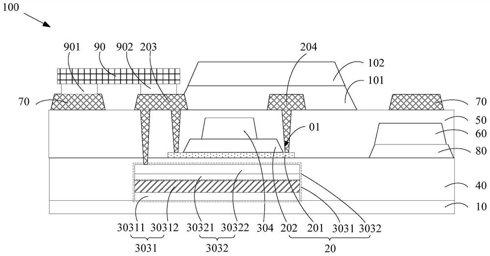
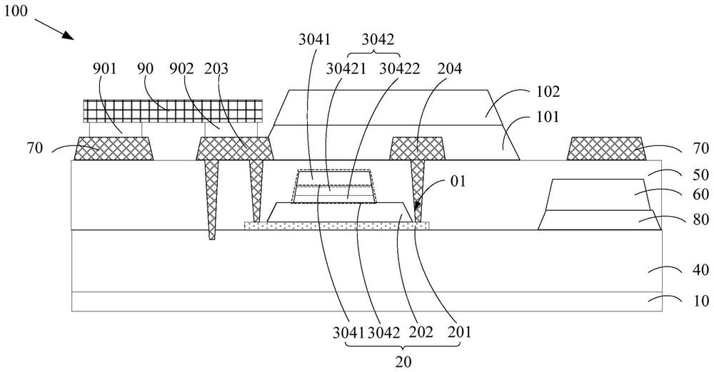
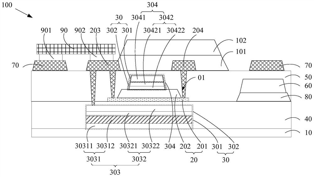
[0047] The technical solutions in the embodiments of the present invention will be clearly and completely described below in conjunction with the drawings in the embodiments of the present invention. Apparently, the described embodiments are only some of the embodiments of the present invention, but not all of them. Based on the embodiments of the present invention, all other embodiments obtained by those skilled in the art without creative efforts fall within the protection scope of the present invention.

[0048] In the description of the present invention, it should be understood that the orientation or positional relationship indicated by the terms "upper", "lower", "closer", "farther away" etc. is based on the orientation or positional relationship shown in the drawings, for example, " "upper" means that the surface is above the object, specifically refers to directly above, obliquely above, or the upper surface, as long as it is above the level of the object; "both sides" o


PUM


Abstract

The invention provides a display panel, a manufacturing method thereof and a display device. The display panel comprises a substrate and a thin film transistor layer, wherein the thin film transistor layer is located on the substrate and comprises an active layer, a metal layer and an anti-reflection layer; the anti-reflection layer is at least located on the side, close to the active layer, of the metal layer; and the reflectivity of the anti-reflection layer is smaller than that of the metal layer. According to the display panel, light irradiated to the active layer can be reduced, the risk of failure caused by performance change of the thin film transistor layer is reduced, and the working stability and reliability of the thin film transistor layer are improved.

Description


Claims


Application Information

Patent Timeline
Owner SHENZHEN CHINA STAR OPTOELECTRONICS SEMICON DISPLAY TECH CO LTD
Why Eureka
Try Eureka