Display device and fabrication method of display device

a technology of display device and fabrication method, which is applied in the direction of identification means, instruments, static indicating devices, etc., can solve the problems of increasing and the inability to form al film, so as to prevent the deterioration of the transparent conductive film and the increase of the fabrication cost of the film forming devi

Active Publication Date: 2005-11-17
PANASONIC LIQUID CRYSTAL DISPLAY CO LTD +1
View PDF15 Cites 0 Cited by
  • Summary
  • Abstract
  • Description
  • Claims
  • Application Information

AI Technical Summary

Benefits of technology

The technical effect of this patented technology is that it allows for better protection against damage caused by cells from reactions on the surface of an optical element used in displays. This results in improved performance and reduced costs compared to traditional methods.

Problems solved by technology

This patent describes different ways to improve the performance of LCD displays. One way involves reducing the loss of light caused by reflection from external sources during use. Another approach involves preventing the etching process itself from causing damage to the underlying layers of the LC films. Additionally, another solution involves providing a protection metal film covering the entirety of the LCO films without exposure to any acidic developers.

Method used


Image

  • Display device and fabrication method of display device
  • Display device and fabrication method of display device
  • Display device and fabrication method of display device

Examples


Embodiment Construction

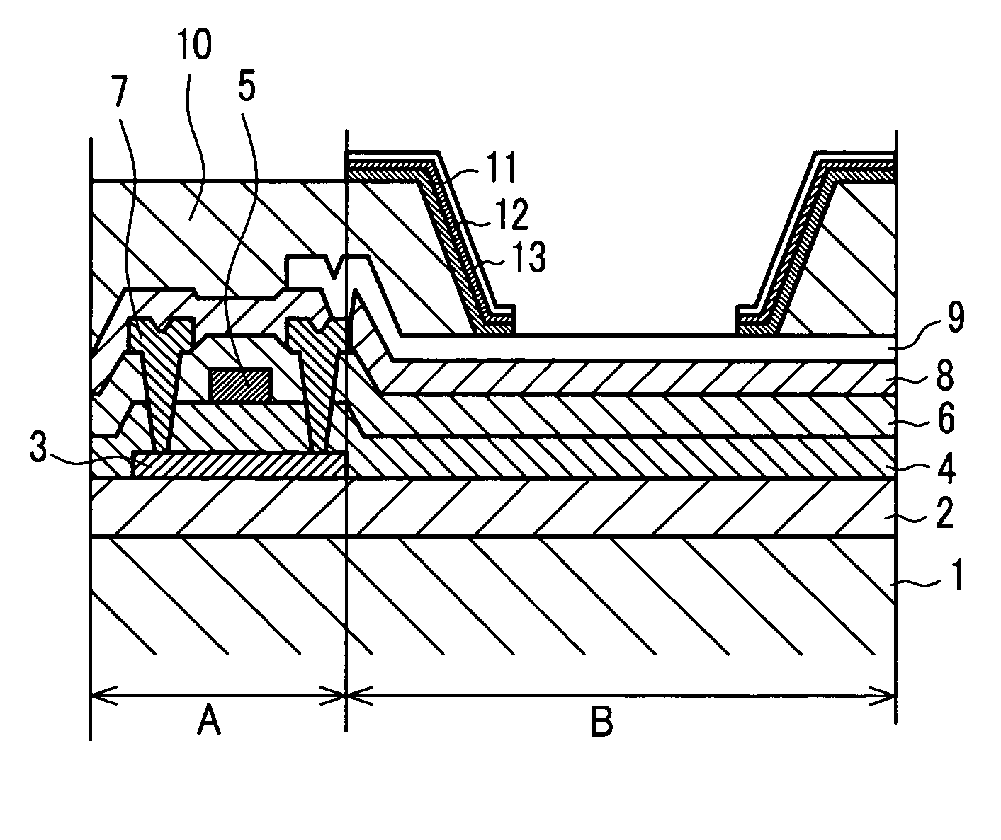
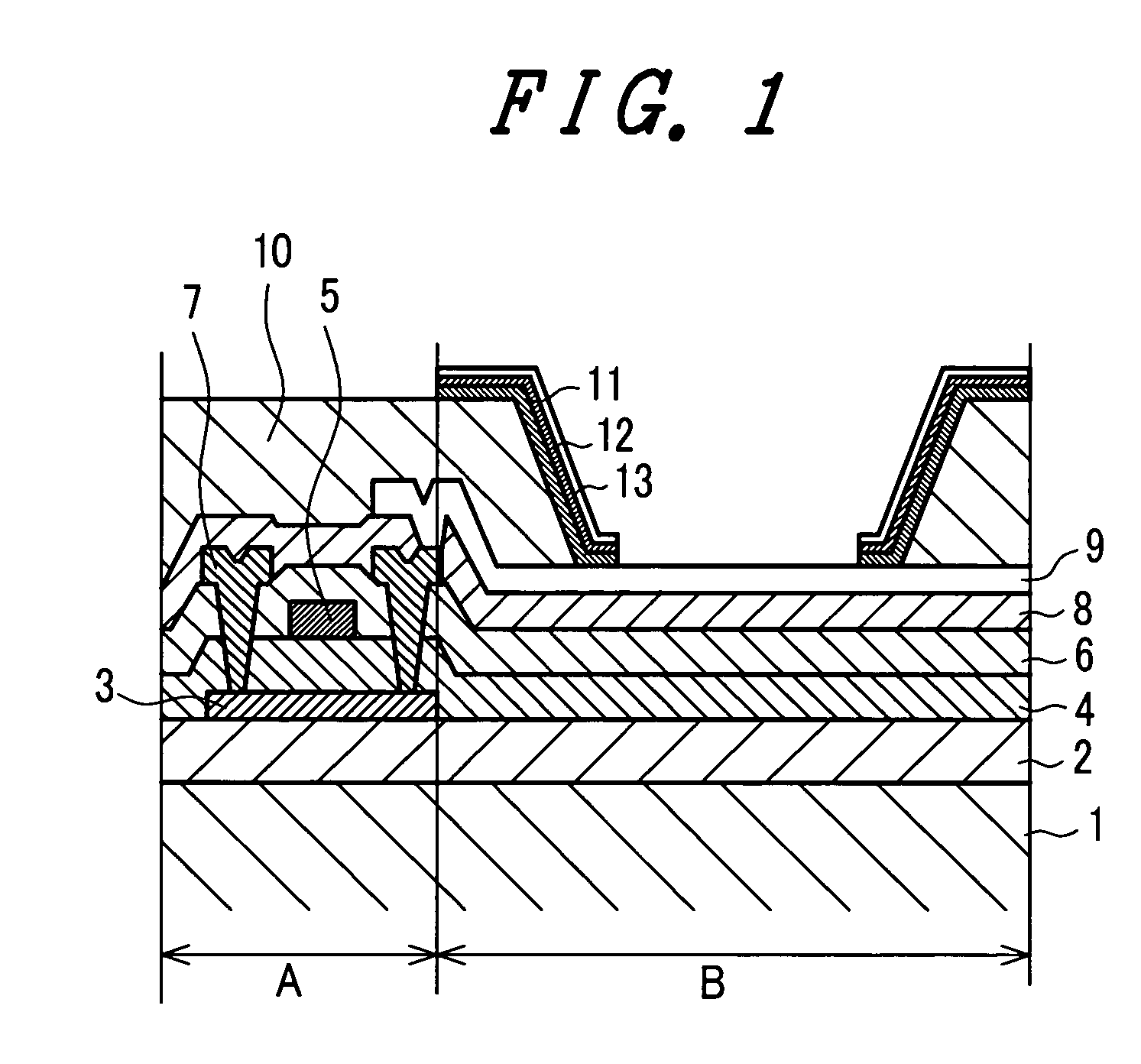
[0044] Hereinafter, an embodiment in which the present invention is applied to a reflective electrode of a partial-transmissive-type liquid crystal display device is explained in detail in conjunction with drawings.

[0045] Here, in all drawings which explain the embodiment, parts having identical functions are given equal symbols and their repeated explanation is omitted.

[0046]FIG. 1 is a cross-sectional view showing the cross-sectional structure of an essential part of the liquid crystal display device of the embodiment of the present invention.

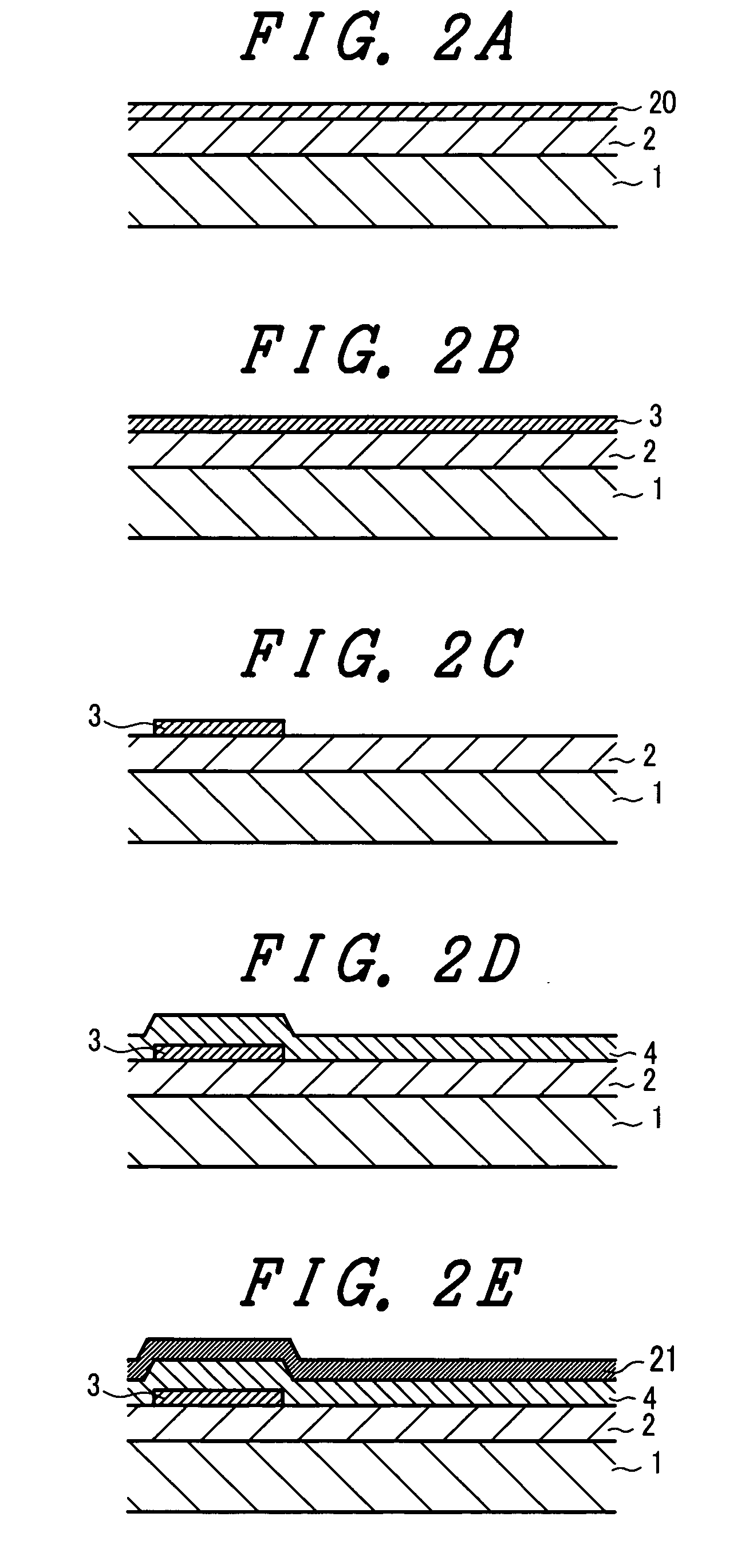
[0047] In the drawing, numeral 1 indicates a glass substrate, numeral 2 indicates a background layer, numeral 3 indicates a polysilicon layer, numeral 4 indicates a gate insulation film, numeral 5 indicates a gate electrode, numerals 6, 8 indicate insulation films, numeral 7 indicates source / drain electrodes, numeral 9 indicates a transparent electrode (ITO film), numeral 10 indicates an overcoat layer (organic insulation film), numeral 11


PUM


Abstract

The present invention provides a display device which can prevent the deterioration of a transparent conductive film attributed to a cell reaction without pushing up a cost of a film forming device. The display device includes a first conductive layer which is formed of a transparent conductive film containing indium oxide as a main component, a conductive background layer which is formed on the first conductive layer, a second conductive layer which is formed of a film containing Al as a main component on the background layer, and a third conductive layer which is formed of the same material as the second conductive layer on the second conductive layer. On an interface between the second conductive layer and the third conductive layer, positions of grain boundaries are arranged discontinuously. Further, the background layer is a film which contains any one of Mo, Ti and Ta as a main component. Still further, the third conductive layer is used as a reflective electrode.

Description


Claims


Application Information

Patent Timeline
Owner PANASONIC LIQUID CRYSTAL DISPLAY CO LTD
Why Eureka
Try Eureka