Semiconductor memory
- Summary
- Abstract
- Description
- Claims
- Application Information
AI Technical Summary
Benefits of technology
Problems solved by technology
Method used
Image

Examples
Example
[0067] 2. First Embodiment
[0068] A semiconductor memory according to the first embodiment of the present invention will be described first.
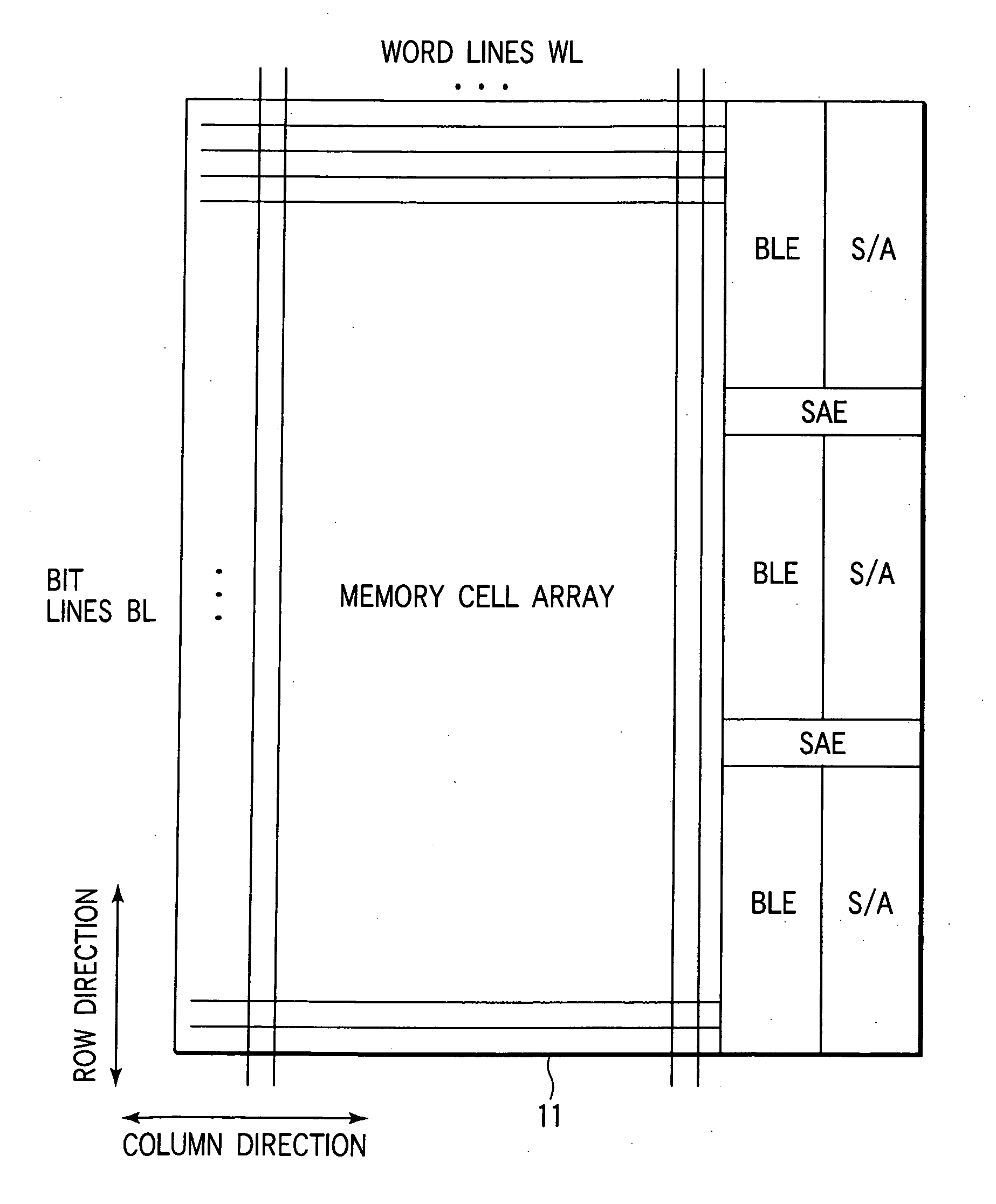
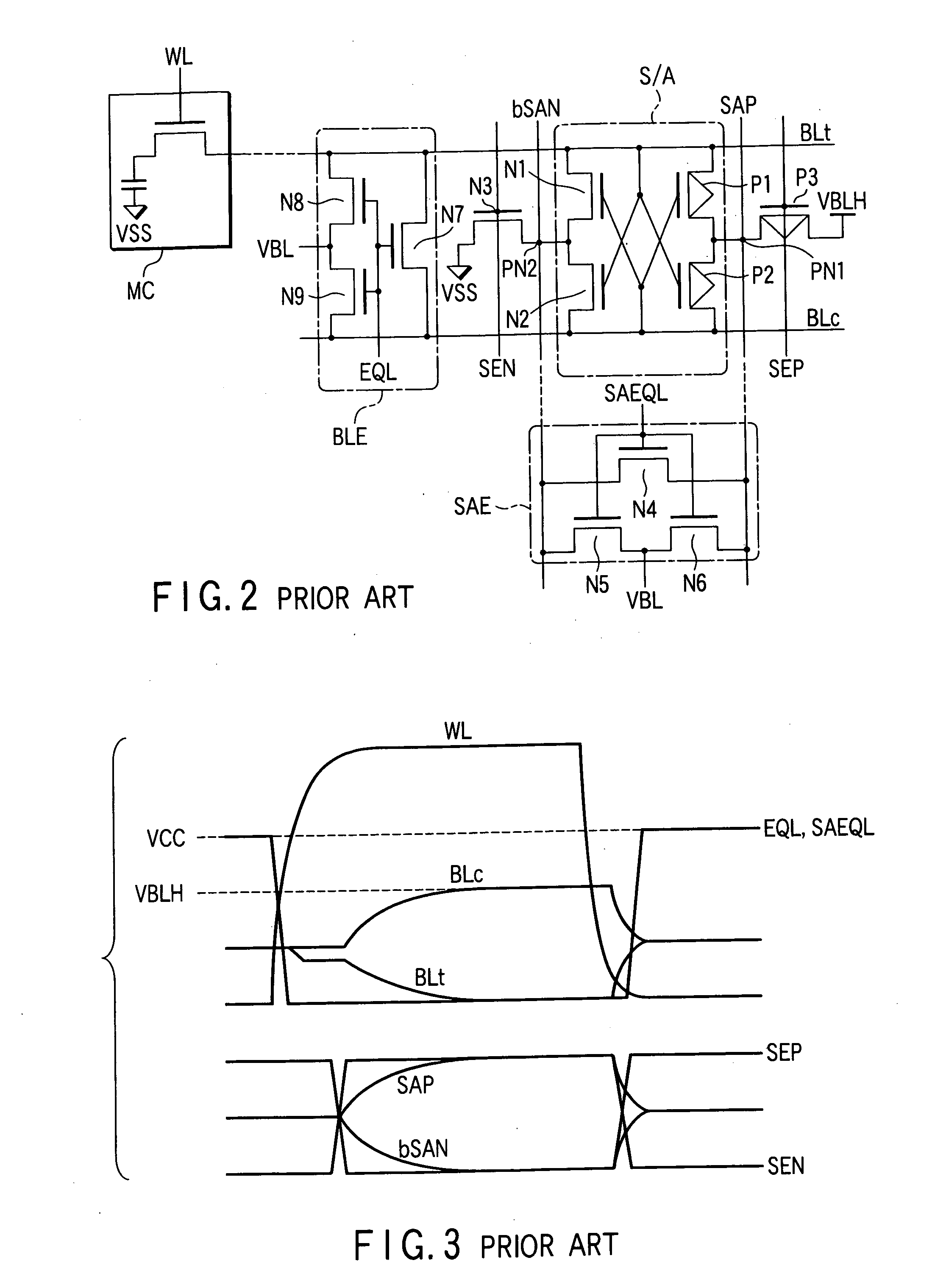
[0069]FIG. 8 shows the layout of the memory cell array portion of a semiconductor memory according to the first embodiment of the present invention. FIG. 9 shows the equivalent circuit of the portion shown in FIG. 8. FIG. 10 shows the meanings of symbols shown in FIG. 9.
[0070] As a characteristic feature of this embodiment, a sense amplifier equalizer SAE is constituted by two types of MOS transistors whose gate oxide films have different thicknesses and, more specifically, VCC type MOS transistors formed in a thick film type Tr area A and VBLH type MOS transistors formed in a thin film type Tr area B.
[0071] This structure corresponds to a structure in which a bit line equalizer BLE is constituted by VCC type MOS transistors formed in the thick film type Tr area A, and a sense amplifier S / A is constituted by VBLH type MOS transistors formed in
Example
[0090] 3. Second Embodiment
[0091] A semiconductor memory according to the second embodiment of the present invention will be described next.
[0092]FIG. 12 shows the layout of the memory cell array portion of a semiconductor memory according to the second embodiment of the present invention. FIG. 13 shows an equivalent circuit of the portion shown in FIG. 12. The transistor symbols in FIG. 10 also apply to FIG. 13.
[0093] In the first embodiment (FIGS. 8 to 10), the sense amplifier equalizer SAE is constituted by the VBLH type MOS transistor N44 and VCC type MOS transistors N55 and N66, whose gate oxide films have different thicknesses. On the other hand, only VBLH-based binary data (VBLH and VSS) is used as the control signal SAEQL.
[0094] In this case, however, the VCC type MOS transistors N55 and N66 having thick gate oxide films are also controlled by the VBLH-based binary data (VBLH and VSS). That is, since the value of the “H”-level potential of the binary data is small, the VCC
Example
[0106] 4. Third Embodiment
[0107]FIGS. 15 and 16 show control signal generation circuits of a semiconductor memory according to the third embodiment of the present invention.
[0108] The third embodiment presumes the semiconductor memory according to the second embodiment. In this semiconductor memory, the sense amplifier equalizer SAE is controlled by two types of control signals SAEQL and SAEQLC.
[0109] When the potential difference between the “H”-level voltage of the control signal SAEQL and that of the control signal SAEQLC increases, and the voltages fluctuate, the potential change timing largely shifts (“L”→“H” or “H”→“L”). This timing is controlled by using level shifters.
[0110] When the change timings of the control signals SAEQL and SAEQLC are controlled using level shifters, the skew between the two control signals SAEQL and SAEQLC can be reduced even when the level of voltage VBLH or VCC fluctuates.
[0111] 5. Device Structure
[0112]FIG. 17 shows the schematic device structu
PUM
 Abstract
Description
Claims
Application Information
 - R&D Engineer
- R&D Manager
- IP Professional
- Industry Leading Data Capabilities
- Powerful AI technology
- Patent DNA Extraction
Browse by: Latest US Patents, China's latest patents, Technical Efficacy Thesaurus, Application Domain, Technology Topic.
© 2024 PatSnap. All rights reserved.Legal|Privacy policy|Modern Slavery Act Transparency Statement|Sitemap