Nitride based semiconductor laser device
- Summary
- Abstract
- Description
- Claims
- Application Information
AI Technical Summary
Benefits of technology
Problems solved by technology
Method used
Image

Examples
Example
2. Second Embodiment
[0090]As to a nitride based semiconductor laser device according to a second embodiment, the difference from the nitride based semiconductor laser device 1 according to the first embodiment will be described.
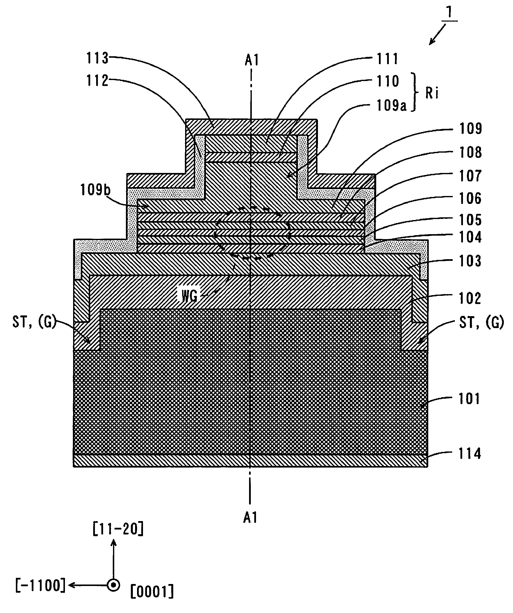
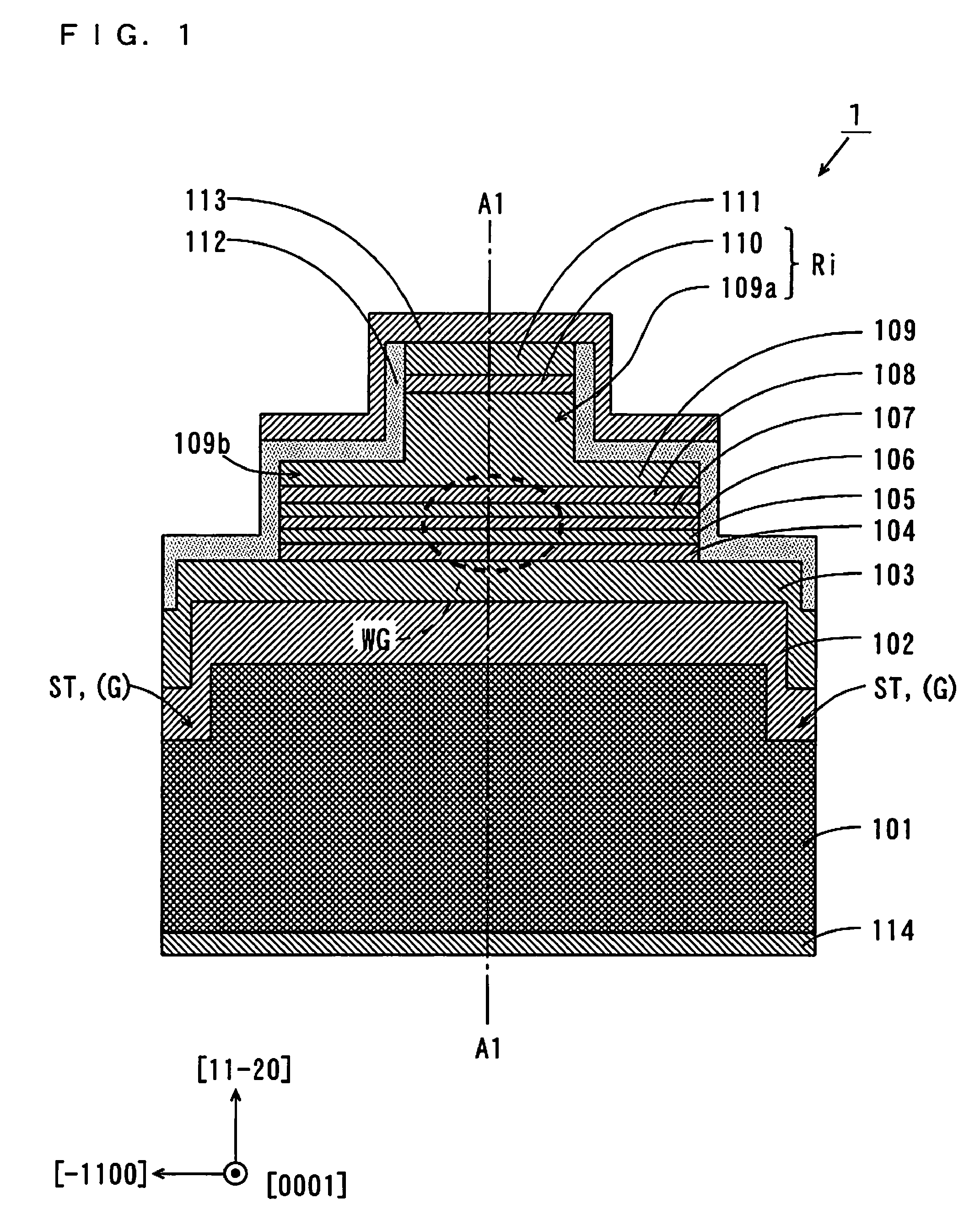
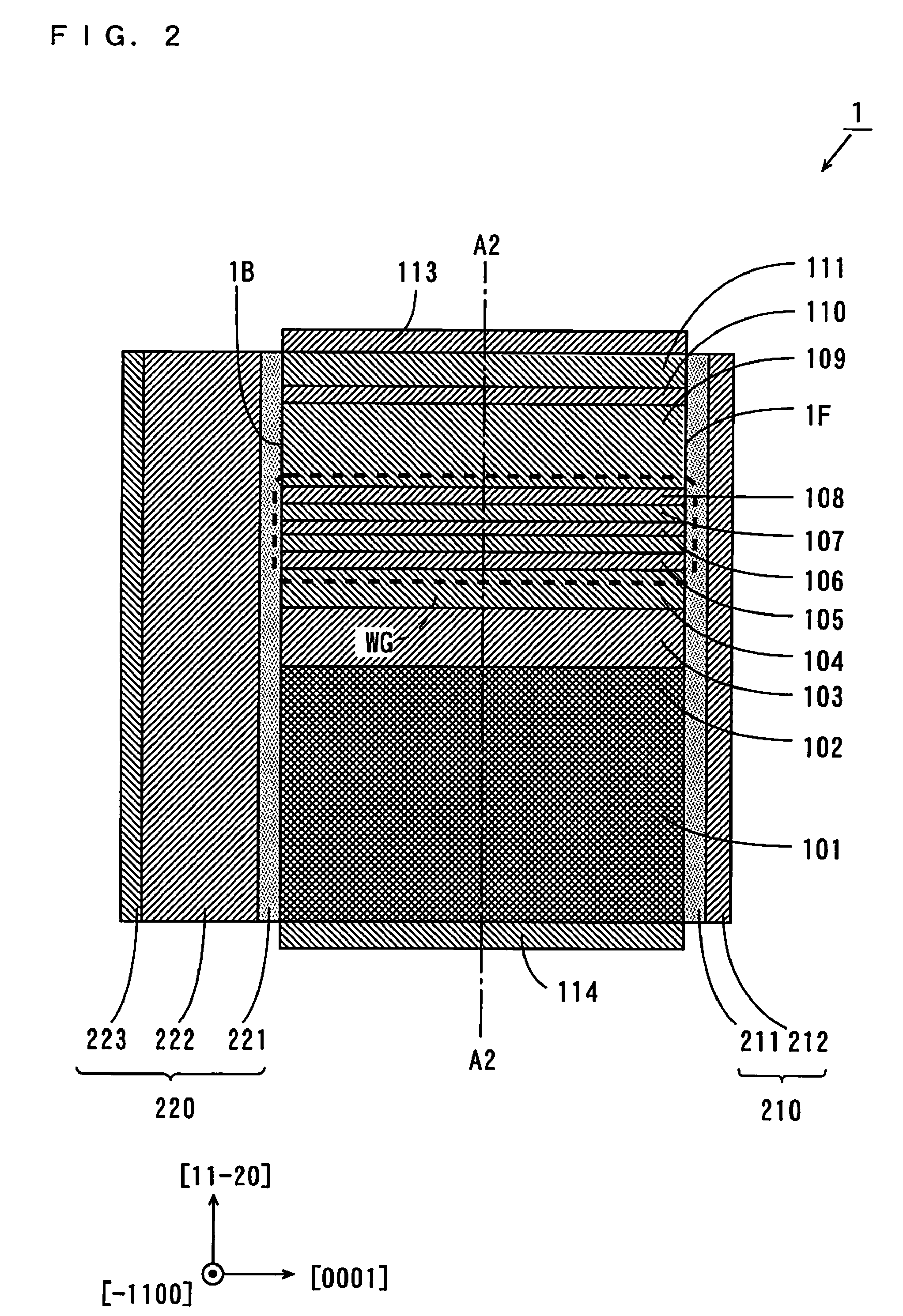
[0091]FIG. 5 is a vertical sectional view of the nitride based semiconductor laser device according to the second embodiment. In FIG. 5, a vertical section of the nitride based semiconductor laser device 1 along a [0001] direction is shown, similarly to the vertical section shown in FIG. 2 in the first embodiment. A vertical section taken along a line A2-A2 shown in FIG. 5 is the same as the vertical section of the nitride based semiconductor laser device 1 shown in FIG. 1.
[0092]A first dielectric multilayer film 210 is formed on a light emission facet 1F of the nitride based semiconductor laser device 1. The first dielectric multilayer film 210 has a structure in which an AlOXNY film (X211a and an Al2O3 film 212a are laminated in this order. Here, the refractiv
Example
3. Third Embodiment
[0096]As to a nitride based semiconductor laser device according to a third embodiment, the difference from the nitride based semiconductor laser device 1 according to the first embodiment will be described.
[0097]FIG. 6 is a vertical sectional view of the nitride based semiconductor laser device according to the third embodiment. In FIG. 6, a vertical section of the nitride based semiconductor laser device 1 along a [0001] direction is shown, similarly to the vertical section shown in FIG. 2 in the first embodiment. A vertical section taken along a line A2-A2 shown in FIG. 6 is the same as the vertical section of the nitride based semiconductor laser device 1 shown in FIG. 1.
[0098]A first dielectric multilayer film 210 is formed on a light emission facet 1F of the nitride based semiconductor laser device 1. The first dielectric multilayer film 210 has a structure in which an AlN film 211b, an AlOXNY film (X212b, and an Al2O3film 213b are laminated in this order. The
Example
4. Fourth Embodiment
[0102]As to a nitride based semiconductor laser device according to a fourth embodiment, the difference from the nitride based semiconductor laser device 1 according to the first embodiment will be described.
[0103]FIG. 7 is a vertical sectional view of the nitride based semiconductor laser device according to the fourth embodiment. In FIG. 7, a vertical section of the nitride based semiconductor laser device 1 along a [0001] direction is shown, similarly to the vertical section shown in FIG. 2 in the first embodiment. A vertical section taken along a line A2-A2 shown in FIG. 7 is the same as the vertical section of the nitride based semiconductor laser device 1 shown in FIG. 1.
[0104]A first dielectric multilayer film 210 is formed on a light emission facet 1F of the nitride based semiconductor laser device 1. The first dielectric multilayer film 210 has a structure in which an AlOXNY film (X211c, an AlOXNY film (X>Y) 212c, and an Al2O3 film 213c are laminated in thi
PUM
 Abstract
Description
Claims
Application Information
 - R&D Engineer
- R&D Manager
- IP Professional
- Industry Leading Data Capabilities
- Powerful AI technology
- Patent DNA Extraction
Browse by: Latest US Patents, China's latest patents, Technical Efficacy Thesaurus, Application Domain, Technology Topic.
© 2024 PatSnap. All rights reserved.Legal|Privacy policy|Modern Slavery Act Transparency Statement|Sitemap