Cross point memory arrays, methods of manufacturing the same, masters for imprint processes, and methods of manufacturing masters

a technology of cross-point memory and arrays, applied in the field of cross-point memory arrays, methods of manufacturing the same, masters for imprint processes, and methods of manufacturing masters, can solve the problems of low integration degree, slow operation speed, and loss of all data stored in the dram

Active Publication Date: 2010-04-15
SAMSUNG ELECTRONICS CO LTD
View PDF11 Cites 29 Cited by
  • Summary
  • Abstract
  • Description
  • Claims
  • Application Information

AI Technical Summary

Benefits of technology

The invention provides an improved way to make memristor devices that can store data. This technology allows for faster processing times and better performance compared to existing technologies like SRAMs.

Problems solved by technology

This patent describes different ways to improve the performance and efficiency of semiconductor memory devices like flash memristors. One way is to use certain techniques called "photomodeling," where a layer of high-density materials can be removed without affecting any previously applied layers. Another technique involves transferring patterned features from a sacrificial layer into a temporary storage location before applying new layers. Additionally, it suggests using nanofluidics to efficiently transfer patterned features during fabrication processes.

Method used


Image

  • Cross point memory arrays, methods of manufacturing the same, masters for imprint processes, and methods of manufacturing masters
  • Cross point memory arrays, methods of manufacturing the same, masters for imprint processes, and methods of manufacturing masters
  • Cross point memory arrays, methods of manufacturing the same, masters for imprint processes, and methods of manufacturing masters

Examples


Embodiment Construction

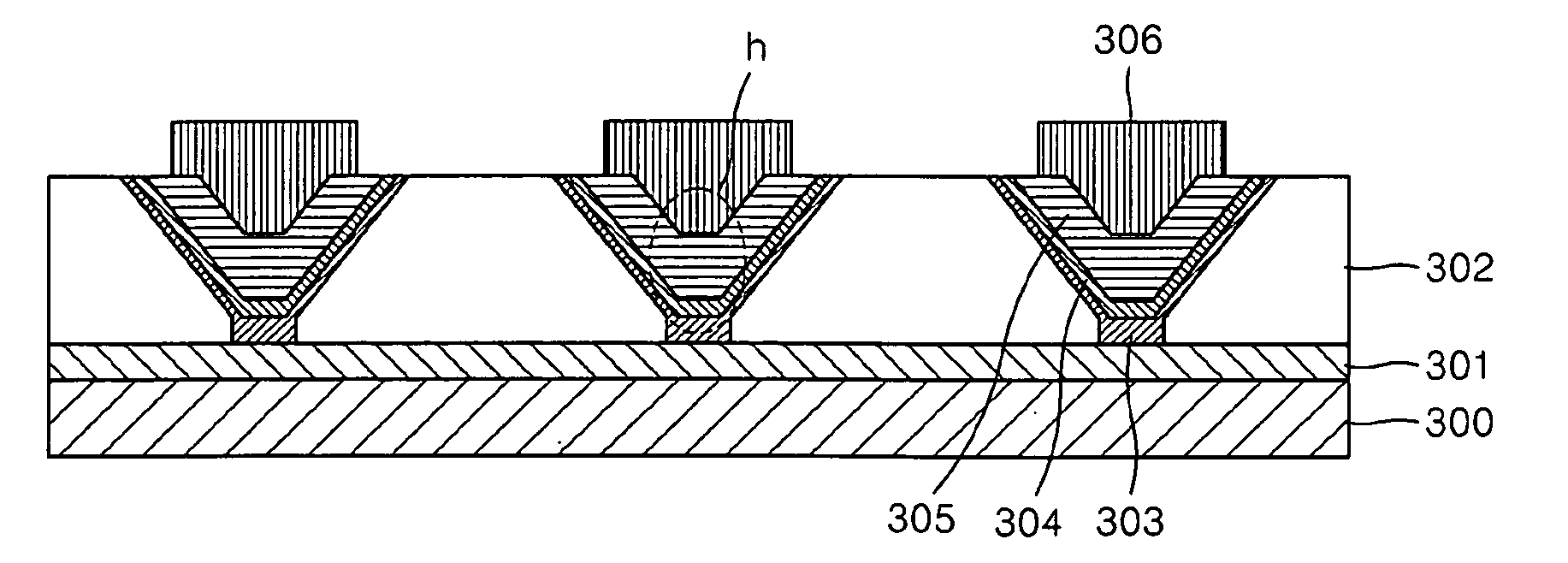
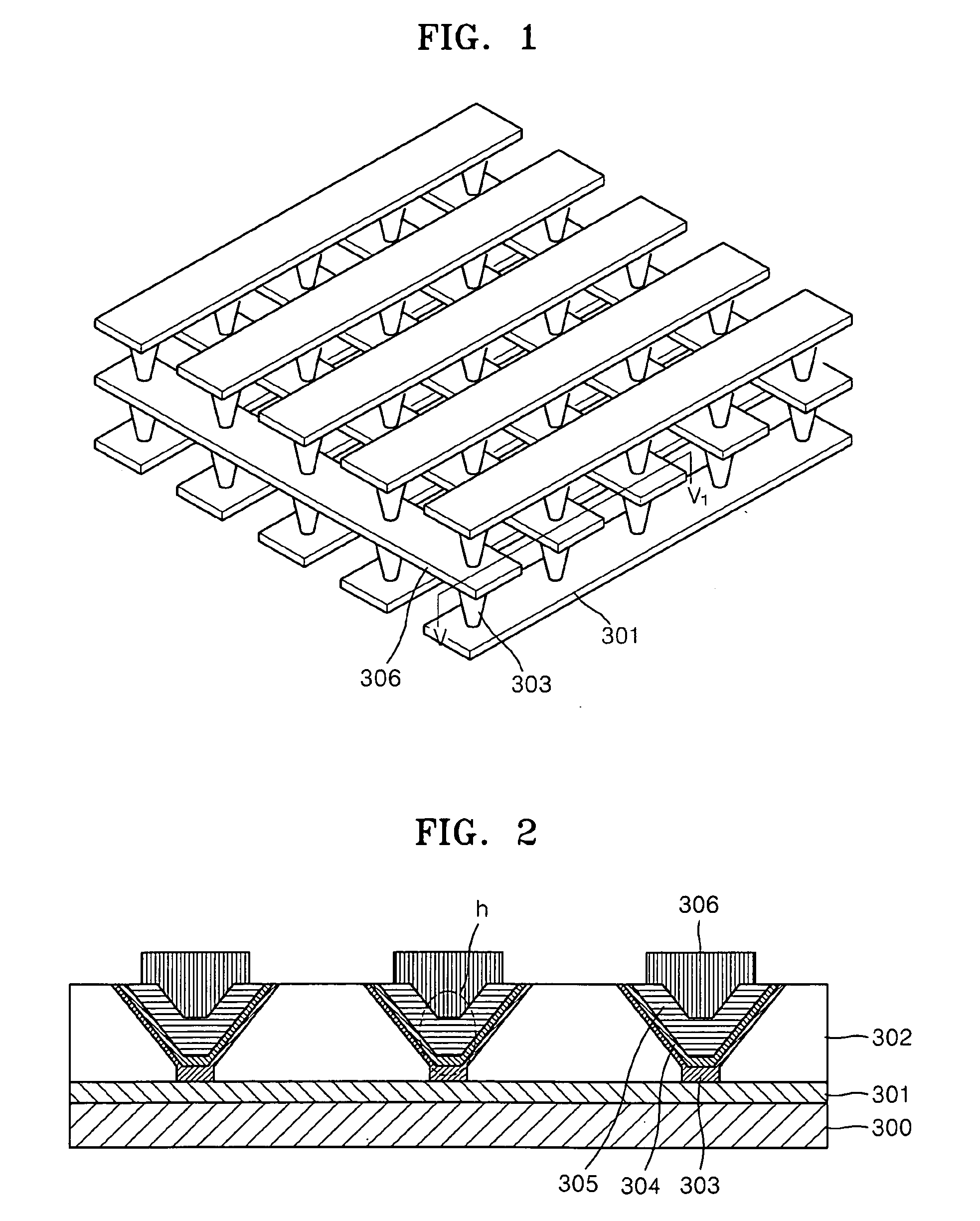
[0034]Various example embodiments will now be described more fully with reference to the accompanying drawings in which some example embodiments are shown. In the drawings, the thicknesses of layers and regions are exaggerated for clarity.

[0035]Detailed illustrative example embodiments are disclosed herein. However, specific structural and functional details disclosed herein are merely representative for purposes of describing example embodiments. Embodiments may, however, may be embodied in many alternate forms and should not be construed as limited to only the example embodiments set forth herein.

[0036]Accordingly, while example embodiments are capable of various modifications and alternative forms, embodiments thereof are shown by way of example in the drawings and will herein be described in detail. It should be understood, however, that there is no intent to limit example embodiments to the particular forms disclosed, but on the contrary, example embodiments are to cover all modif


PUM

PropertyMeasurementUnit
Electrical resistanceaaaaaaaaaa
Sizeaaaaaaaaaa
Shapeaaaaaaaaaa

Abstract

A cross point memory array includes a structure in which holes are formed in an insulating layer and a storage node is formed in each of the holes. The storage node may include a memory resistor and a switching structure. The master for an imprint process used to form the cross-point memory array includes various pattern shapes, and the method of manufacturing the master uses various etching methods.

Description


Claims


Application Information

Patent Timeline
Owner SAMSUNG ELECTRONICS CO LTD
Why Eureka
Try Eureka