Semiconductor recording device
a recording device and semiconductor technology, applied in the field of semiconductor recording devices, can solve the problems of writing error propagating to the already written first page, error propagating to the first page, and writing error, so as to prevent the propagation of writing error due to cell sharing, prevent the propagation of writing error, and prevent the effect of cell sharing
- Summary
- Abstract
- Description
- Claims
- Application Information
AI Technical Summary
Benefits of technology
Problems solved by technology
Method used
Image

Examples
embodiment 1
[0061]FIG. 4 shows a configuration view of a semiconductor recording device according to embodiment 1 of the present invention. In the present embodiment, an interface 1 is an interface for receiving a command and data from a host apparatus not shown in the drawing and transferring the data.
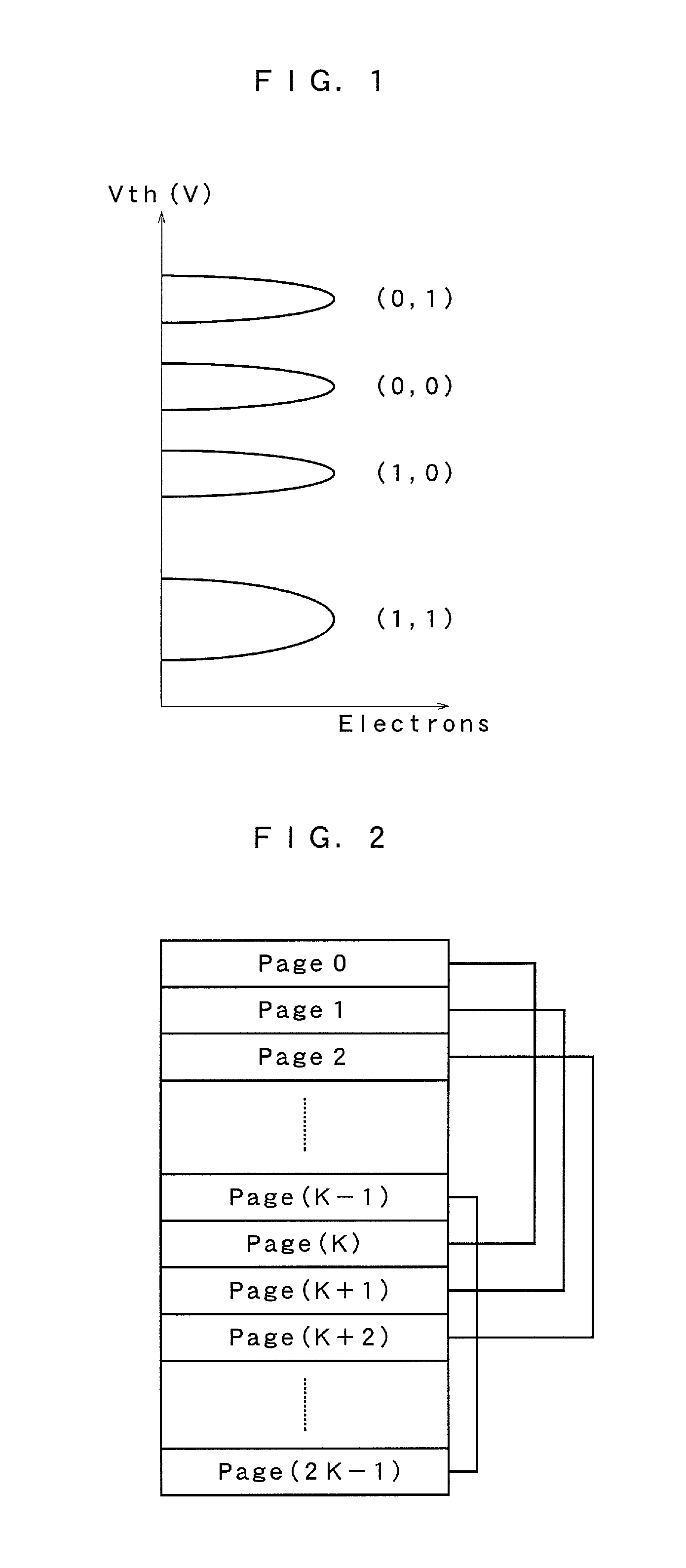
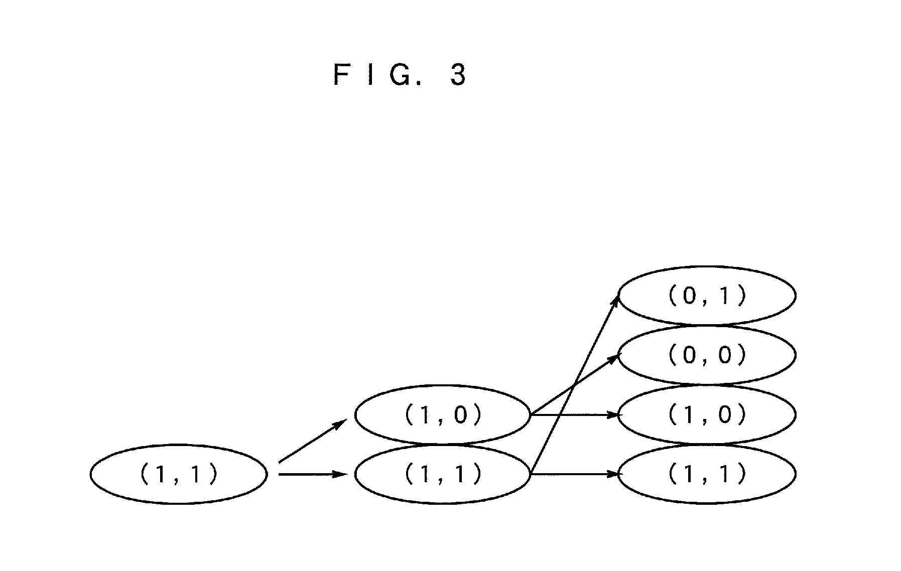
[0062]When receiving a write command from the host apparatus, a first ECC generator 2 (hereinafter simply referred to as an ECC generator 2) adds an error correction parity to received writing data. In more detail, an ECC parity of M words (M is a natural number) is added to N words extracted at intervals of A words in the inputted data of (A*N) words (A and N are natural numbers) to generate A number of the first ECC codes of (N+M) words. Meanwhile, the ECC parity is a code having a function of error correction. Here, in the present embodiment, the explanation will be made assuming that N is four and M is one. In addition, ECC parity is generated to at least the data of a first page of a memory cel
modified example
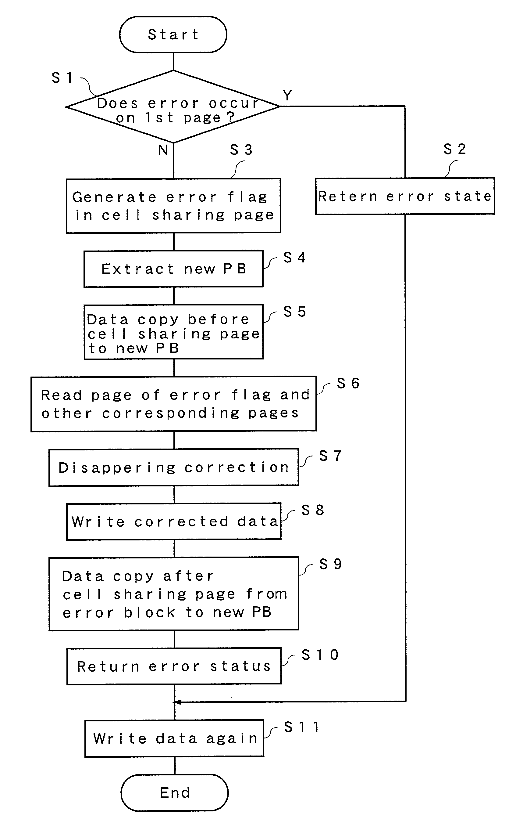
[0079]Next, a modified example of the present embodiment will be explained. This modified example is a case where the information of the cell sharing in a physical block is not disclosed. Accordingly, in this modified example, the ECC generator generates the ECC parities of all pages. Referring to FIG. 9, a process of this case will be explained. In (9-1) of FIG. 9 shows that a writing error occurred in the writing of page (K+1). It is not known whether page (K+1) is the first page or the second page and that the page is in the relation of cell sharing with which page. However, if the second page, the first page being in the relation of cell sharing with page (K+1) is included in page 0 to page K before it. FIGS. 9(9-2) and (9-3) are explanation views in the case of recovering the error occurrence block, FIG. 9(9-2) is a physical block in which the error occurred, and FIG. 9(9-3) is a new physical block after recovering the data. In the process of this case, the error flag generator 7
embodiment 2
[0084]Next, using FIG. 10, a semiconductor recording device according to embodiment 2 of the present invention will be explained. The present embodiment improves an error resistance in the reading in addition to an error correction in the writing. In FIG. 10, an output of the data distributor 3 is given to the second ECC generators 11a to 11e. The second ECC generators 11a to 11e generates the ECC parity to the distributed data, and sets the ECC parity and data, that is, the ECC code in units of page. The output of the ECC is directly given to the data writers 4a to 4e. In addition, outputs of the data readers 12a to 12e are given to the data recovering part 9 via second ECC correctors 13a to 13e. When an error occurred and the error is correctable, the second ECC correctors 13a to 13e give the data after the correction based on the ECC parity in units of page generated by the second ECC generators 11a to 11e. The data readers 12a to 12e read the data related to an address included in
PUM
 Abstract
Description
Claims
Application Information
 - R&D Engineer
- R&D Manager
- IP Professional
- Industry Leading Data Capabilities
- Powerful AI technology
- Patent DNA Extraction
Browse by: Latest US Patents, China's latest patents, Technical Efficacy Thesaurus, Application Domain, Technology Topic.
© 2024 PatSnap. All rights reserved.Legal|Privacy policy|Modern Slavery Act Transparency Statement|Sitemap